


6-Layer vs. 4-Layer: When Does the Signal Integrity Justify the Cost?
 View
View
Every PCB designer hits the same wall: budget constraints versus performance needs. For most simple projects, the standard 4-layer board (Signal-GND-PWR-Signal) is the ideal starting point. It's inexpensive, easily manufactured, and sufficient for low-speed analog and simple digital logic.
But as soon as your design incorporates modern high-speed interfaces, think USB 3.0, DDR3, or PCIe, the landscape changes. Those extra layers increase performance and reduce risk, but when is that cost increase (often 30–50%) truly justified?
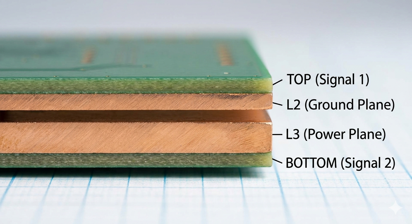
The starting point: A classic 4-layer stackup (SIG-GND-PWR-SIG). Cheap, but limited.
When 4-Layers Fail the Signal Integrity Test
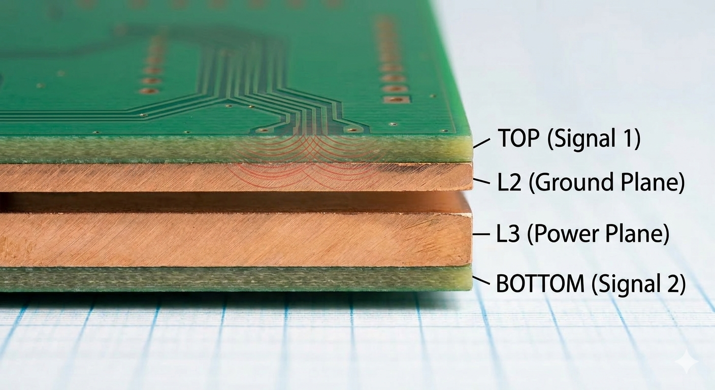
Signal Integrity (SI) issues, crosstalk, impedance mismatch, and power delivery noise, arise when traces have no reference. A 4-layer board provides one internal ground reference plane.
If you route high-speed differential pairs (like the USB signals shown below in Image) on the TOP layer, they have L2 GND for a return path. That seems fine. However, as your routing complexity increases, the tight trace widths and strict spacing required to maintain impedance on 4-layer boards are extremely difficult to manufacture. They start to couple, causing crosstalk and making controlled impedance a bottleneck, increasing manufacturing costs and risk. This visual congestion highlights where the SI problems begin.
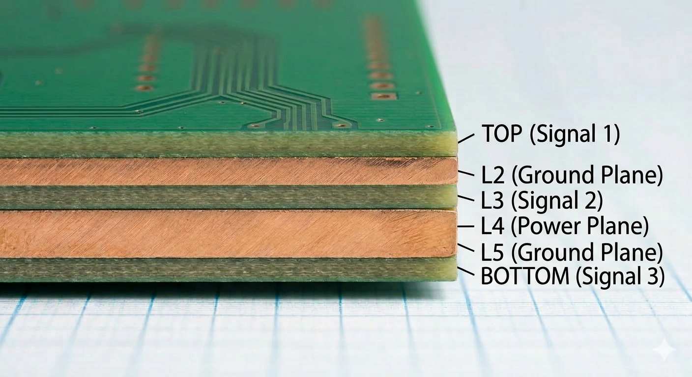
The 6-Layer Solution
The third image will show a cross-section of a 6-layer board, explicitly showing how it solves the issues from Image 2.
It will feature the core stackup with two additional internal layers. It must show a dedicated internal solid ground reference plane (e.g., L2) positioned directly below the sensitive TOP (Signal 1) layer, perfectly shielding the high-speed differential pair from Image 2. This diagram will use clean labels (TOP, L2-GND, L3-SIG, L4-PWR, L5-GND, BOTTOM) and maintain the exact professional diagram style, lighting, and grid paper background seen in Image 1 and Image 2.
The Seamless Solution: EasyEDA Pro + JLCPCB
Transitioning from 4 to 6 layers can feel like a leap, but the EasyEDA Pro and JLCPCB ecosystem turns it into a simple workflow. Using the Layer Manager in EasyEDA Pro, you can instantly upgrade your stackup and define dedicated internal planes.To ensure your high-speed signals stay clean, you can use the JLCPCB Impedance Calculator to get precise trace widths for your 50 ohm or 100 ohm lines, which you then plug directly into your EasyEDA Design Rules.
Sign In Or Register Comment after
No comments yet. Be the first to comment!