


Evaluating JLC’s Lead-Free SMT Process for Medical Prototypes.
 View
View
For medical electronic prototypes, the stakes are significantly higher than for consumer gadgets. Reliability, biocompatibility, and regulatory compliance (like RoHS) are non-negotiable.When you evaluate JLCPCB’s Lead-Free SMT process for a medical application, you are looking at a system designed to meet RoHS (Restriction of Hazardous Substances) standards while maintaining high precision.
1. The Chemistry: Lead-Free (RoHS) Solder
Medical devices must be Lead-Free to prevent toxic heavy metals from entering clinical environments.
- The Alloy: JLCPCB typically uses SAC305 (96.5% Tin, 3.0% Silver, 0.5% Copper) for their lead-free process.
- The Challenge: Lead-free solder has a higher melting point and lower "wettability," meaning the solder doesn't flow as easily.
- Medical Impact: SAC305 joints are generally stronger and more resistant to "creep" (deformation under stress), which is vital for devices that might undergo vibration or thermal cycling in a hospital setting.
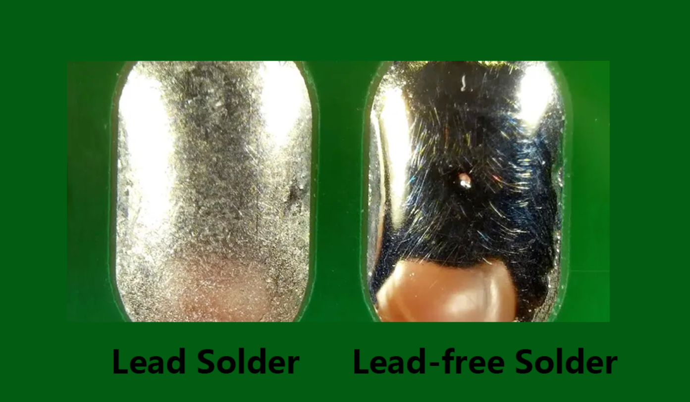
[!IMPORTANT]
Because lead-free solder is less shiny than leaded solder, a "dull" joint in a medical prototype isn't necessarily a "cold" joint—it’s just the nature of the alloy.
2. Precise Component Placement (Pick and Place)
For medical prototypes involving tiny sensors or BGA/QFN packages, manual placement is too risky.
- Automation: JLC uses high-speed Yamaha and Panasonic Pick-and-Place machines. These machines use high-resolution cameras (Vision Systems) to align components with micrometer precision.
- Medical Accuracy: This ensures that parasitic capacitance and inductance, which can ruin the readings of a sensitive medical analog front-end (AFE), are minimized by perfectly centering components on their pads.
For medical electronic prototypes, the evaluation of an SMT process centers on three pillars: Compliance (RoHS), Reliability (Solder Integrity), and Traceability.
When using JLCPCB for medical prototypes, you are essentially leveraging an industrial-scale automated line for small-batch runs. Here is how their lead-free process stands up to medical-grade requirements.
1. RoHS Compliance & Material Safety
Medical devices must be Lead-Free to ensure they are non-toxic in clinical environments.
- The Alloy: JLCPCB uses SAC305 (96.5% Tin, 3.0% Silver, 0.5% Copper). This is the gold standard for lead-free soldering.
- The Finish: For medical boards, you should pair lead-free SMT with an ENIG (Electroless Nickel Immersion Gold) surface finish. This provides a perfectly flat surface for tiny medical sensors and prevents oxidation over long-term use.
2. High-Density SMT: The "Medical-Grade" Machine
Medical prototypes often use tiny components (like 0201 or 0402 resistors) to save space.
- Pick-and-Place (P&P): JLC uses advanced Yamaha and Panasonic machines with Vision Alignment. Before placing a component, a high-resolution camera checks the pads and the component's center.
- Precision: This is critical for medical ICs like 24-bit ADCs or tiny BLE (Bluetooth Low Energy) modules, where a misaligned pad could introduce parasitic noise or a bridge.
3. Verification: AOI and X-Ray
For medical prototypes, "it looks okay" is not enough. You need Automated Inspection.
- AOI (Automated Optical Inspection): A series of cameras and lights sweep the finished board. In the lead-free process, AOI is tuned to recognize the dull, grainy appearance of SAC305 as a "good" joint, rather than a "cold" joint.
- X-Ray: For QFN and BGA packages (common in high-end medical microcontrollers), JLC uses X-Ray Inspection. This is the only way to catch hidden shorts or "voids" under the chip.
- Medical Impact: In a diagnostic device, a single void in a thermal pad can cause the processor to overheat and fail during a surgery or test.

Sign In Or Register Comment after
No comments yet. Be the first to comment!