


Mastering EasyEDA Pro: Top 10 Features You Aren't Using
 View
View
You can’t master EasyEDA Pro by simply putting down some components, clicking on generate gerbers and moving on to the next project. This is the basic level of mastery. You will experience your biggest gains at the next level due to the features within this program that are potentially “hidden”, but can add so much value to your designs, and sanity!
First, start with Custom Design Rule Checks (1). Default design rule checks are just considered to be “cross your fingers and hope for the best”. If you set these up correctly, you will create an environment for yourself where you can catch mistakes before making an expensive coaster out of your PCB. Next, use the built-in real-time 3D visualization (2) tool to answer the age-old question of “does this fit?” before your enclosure gives you an answer of “no”.
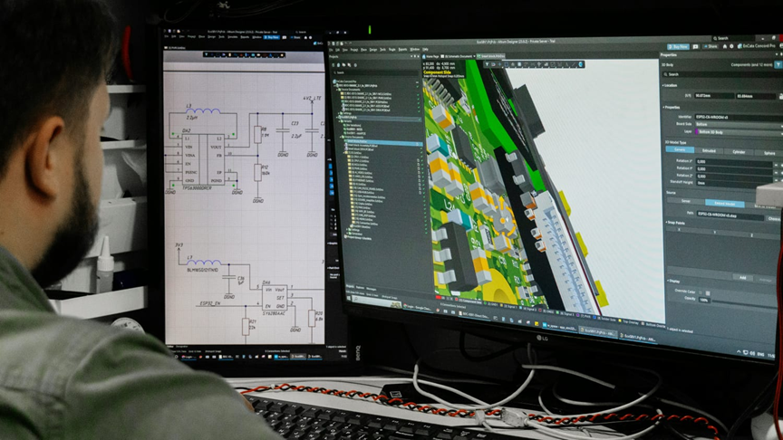
3D visualization Tools(conceptual)
Next, utilize the built-in signal integrity tools (3). While these tools may not provide precision laboratory results, they will provide you with enough information to notice when your high-speed traces look like chaos noodles. Pair these two features with differential pair routing (4) and length tuning (5), and all of a sudden your USB and high-speed traces no longer have a mind of their own.
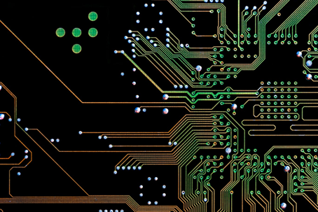
PCB Design close-up
Last, the Footprint Manager (6) is also a hidden gem, because there isn't a better way to humble yourself than from a mismatched footprint. Meanwhile, using the version history (7) feature will also save you from your own “just one little change” disasters.
Don’t forget to include LCSC integration (8) as part of your processes; this is another chance to validate whether your design is manufacturable from a parts perspective. You should also use** panelization tooling (9)to reduce production costs, plus you should also use the Gerber viewer (10) as your final check for assuring you are going to send the right files to manufacturing.
By using these items together, EasyEDA Pro will transition from being just a tool, and become a design partner that will occasionally help you avoid heartache.
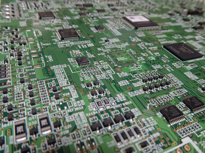
Printed Circuit Board close-up
Sign In Or Register Comment after
No comments yet. Be the first to comment!