


How to Design a PCB for 20A Current Without Melting Traces
 View
View
Designing a PCB for 20 A shouldn't be left to chance; it’s the result of sound engineering regarding heat, resistance, and copper management.
The first guiding principle is the importance of trace sizes. For example, according to IPC guidelines, a 20A trace on an external conductor (2 oz of copper per square foot) experiencing a temperature rise of 10 °C will require approximately 2.6-3 mm in width. Anything narrower than 2.6 mm will eventually heat the trace enough to melt, rendering it a fuse.
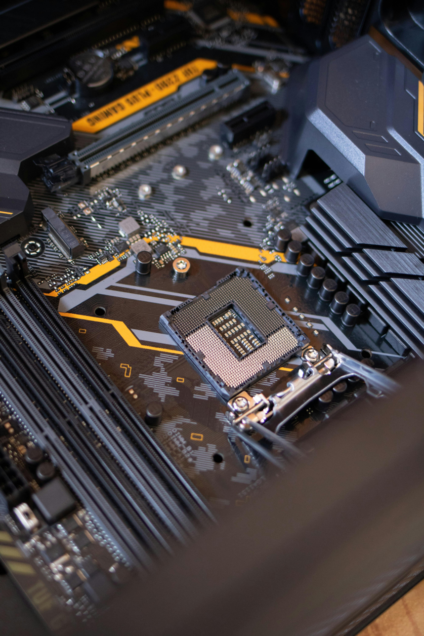
PCB copper traces close-up
The second principle is that you should always use the largest-gauge copper conductor you can. For example, if you are switching from 1oz copper conductors at 20A to 2 oz or larger-gauge copper conductors, you will substantially reduce the resistance and heat generated by the conductor. Think of this as increasing the water pipe's diameter and reinforcing the walls.
The third principle is to avoid the use of thin trace conductors completely; instead use copper pours or planes. Distributing the current over a larger surface area improves thermal performance by reducing hot spots and increasing the area available to dissipate excess heat, thereby also reducing voltage drop.
The fourth guideline is to use the shortest and most direct trace routing possible. Any time you lengthen a trace, you will substantially increase the resistance (R= ρL/A), which in turn will increase the heating and the voltage drop. Therefore, try to keep your high current paths as short as possible.
The fifth suggestion is to consider the use of multiple vias when routing power as a single via can cause a current bottleneck; Thus, to properly share the load and dissipate heat create multiple vias in parallel when the current load permits.

High-current PCB / power electronics
Finally, be aware of your thermal strategy. External traces will have better cooling characteristics than internal traces, and also the use of airflow and copper planes can greatly enhance the amount of current a trace can carry.
What’s the takeaway? When designing for 20A isn’t making sure there is a single “perfect trace width”; it’s increasing cross-sectional copper and minimizing resistance throughout the entire length of the trace. By doing this, your board should stay cool, perform well, and not melt.
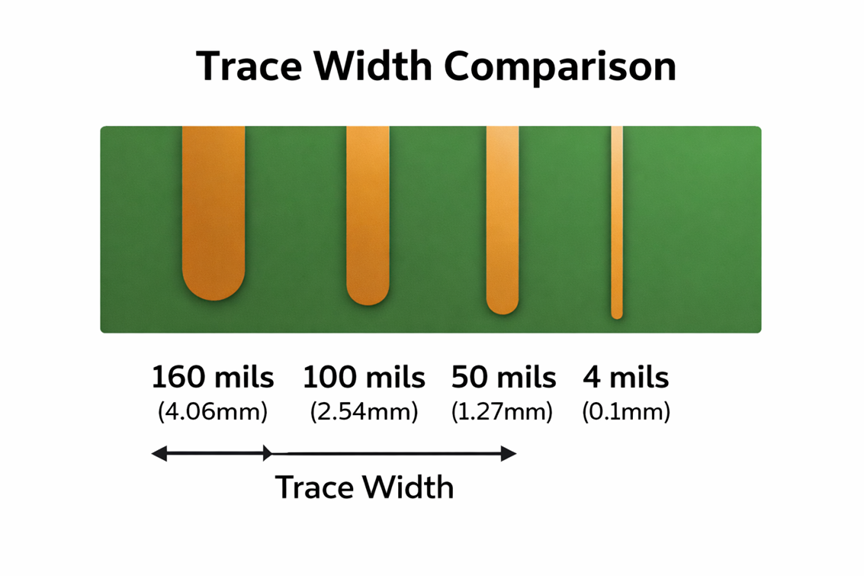
Trace width comparison
Sign In Or Register Comment after
No comments yet. Be the first to comment!