


Why I Always Use 4-Layer Boards for High-Speed Logic
 View
View
I typically use four-layer PCB designs for high-speed digital logic designs, not for aesthetics, but to minimize problems down the road.
There are significant benefits to using four-layer PCBs, of which dedicated planes are the most obvious. A four-layer stack provides both a solid ground plane and a power plane, which significantly reduces noise and provides low-impedance return paths to the components in a circuit. The high-frequency returning paths will be through their signal traces as well as through the ground returning to it. Keeping this return path as continuous as possible using the ground plane keeps these paths very short, which will reduce the total size of the loop and therefore reduce the EMI generated.
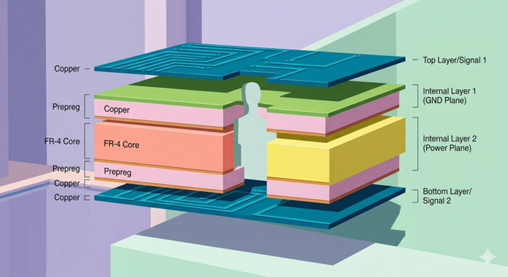
4-layer PCB stackup diagram
The second benefit of using four-layer PCBs is signal integrity. With four-layer boards, the controlled layer spacing allows for better impedance control and reduced signal reflections. Signal integrity is important with very fast signal edges, even in “moderate” MHz designs, as rise time can create problems even at relatively low frequencies. In comparison to a simple two-layer board, where signals and return paths may compete for routing space, the four-layer PCB will have more consistent routing guidelines as well.
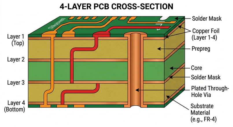
PCB internal layers / cross-section
In addition to using a consistent routing approach, the benefits of routing efficiency are significantly improved on a four-layer PCB due to having two outer signal layers and two inner planes available for routing. This substantially reduces the number of compromises such as reduced crossovers, long routing detours, or unwanted coupling between signals.
Last, but definitely not least, having a dedicated power plane significantly helps with power distribution. The dedicated power plane provides reduced voltage drop, and when placed close to the ground plane for decoupling, it creates a significant amount of inherent capacitance, which helps to stabilize the supply rails.
In the past, cost was an obstacle to using a 4-layer PCB, but now many manufacturers, particularly JLCPCB, are providing 4-layer PCBs at such low prices that the performance improvement almost rarely justifies the increased cost.
This creates cleaner signals, is less likely to cause EMI, and reduces the amount of time spent debugging the board.
Close-up of dense PCB traces
Sign In Or Register Comment after
No comments yet. Be the first to comment!