


The Art of Via Stitching: Improving Thermal and RF Performance
 View
View
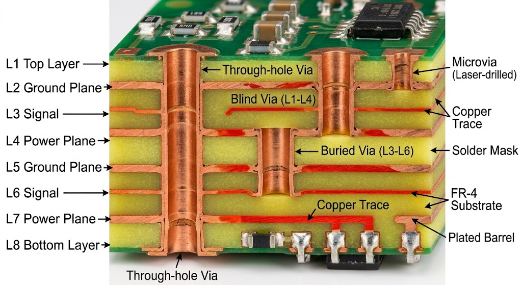
Multilayer PCB showing vias
Via stitching is a simple yet powerful way to improve your PCB design. Adding multiple ground vias along traces and adjacent to the edges will give you a low-impedance path between layers. This will help improve the flow of return current, reduce EMI, and help confine RF signals, especially for designs with high frequencies.
Stitched vias also aid in the thermal management of your board by creating a transfer path for heat generated by hot components to the internal planes of the PCB. They are typically used under power devices and next to ground planes.
The most important factor to consider when designing stitched vias is their spacing. You should have enough vias together to provide an effective low-impedance path (usually λ/10 at RF frequencies), but their total distance apart cannot be excessive.
With proper implementation, via stitching improves thermal performance as well as signal integrity.
Sign In Or Register Comment after
No comments yet. Be the first to comment!