


How to Properly Generate Gerber Files for JLC in 5 Different EDA Tools
 View
View
Making clean Gerber files is the final stage between your design and a successful build. While there are different workflows with the use of the different tools used for generating Gerber files, the main fundamentals are always consistent - specifically for preparing files for JLCPCB.
First, go to KiCad. Then, Use the Plot menu. Typically, various layers must be output from the Plot menu in RS-274X format. You will not have a drill layer combined with your other layers when making the Gerber files. It’s extremely important that you process your drill layer independently of your other layers.
Once the Gerber files have been generated, you should also check the Gerber files for plotting accuracy using the internal viewer.
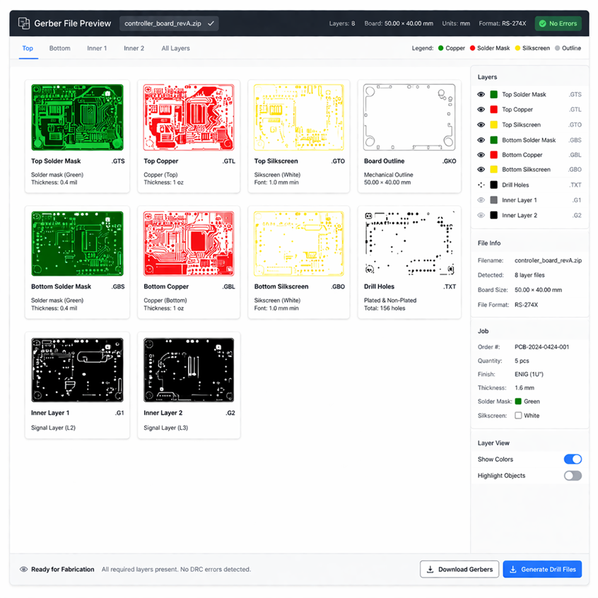
Gerber file preview / PCB layers visualization
In EAGLE, using a CAM Processor will allow users to load in a standard job Gerber file and generate all required layers. Be sure to double-check names when renaming layers to avoid any confusion.
Though EasyEDA does not create GERBERS by hand, users must still review output layers and preview before submitting order.
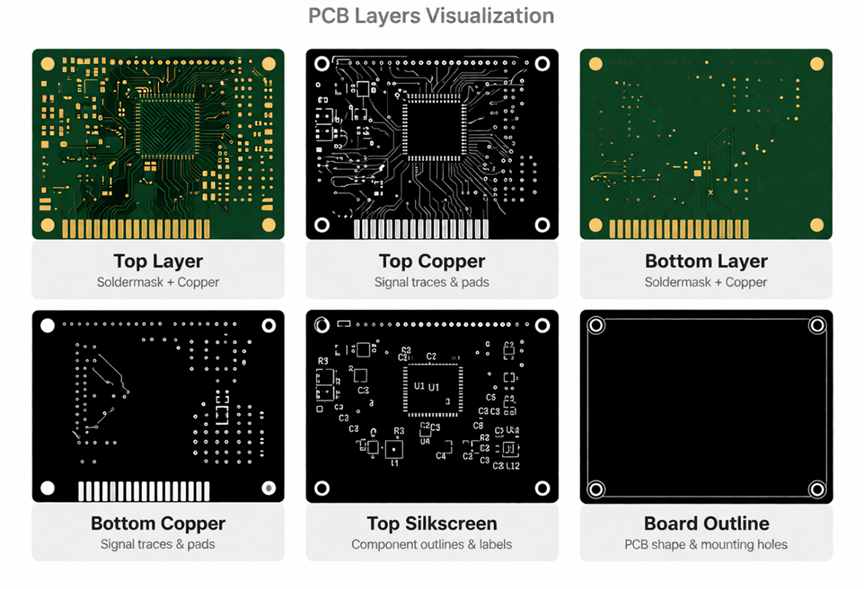
Gerber file preview / PCB layers visualization close-up
If using OrCAD, you will need to use the Manufacture → Artwork process. You will define the film output for the layers you require, as well as when you export to the NC drill files.
Regardless of the software you are using, there are three main steps that you will always need to do in order to prepare your final output – always include all of the layers required, always know what units you are using, and always verify the generated output prior to submitting it. A quick verification in a Gerber viewer may help prevent an expensive mistake in fabrication.
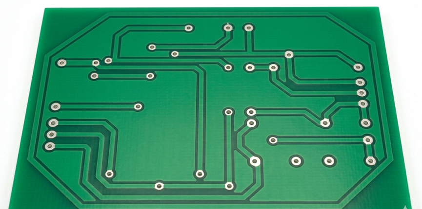
PCB with a green solder mask coating applied
Sign In Or Register Comment after
No comments yet. Be the first to comment!