


Introduction to Microwave Engineering for PCB Designers
 View
View
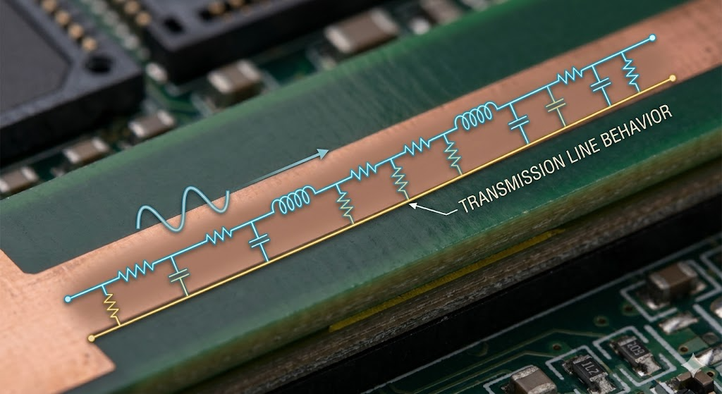
High-frequency circuit board design (microwave design) applies not only to radio frequency circuit board design engineers, but also to today's designers of circuit boards. Circuit board, or PCB, designers use microwave design principles as they reach frequencies of hundreds of MHz or more, where traces on Printed Circuit Boards (PCBs) are no longer behaving as simple wire connections, but will instead function as transmission lines.
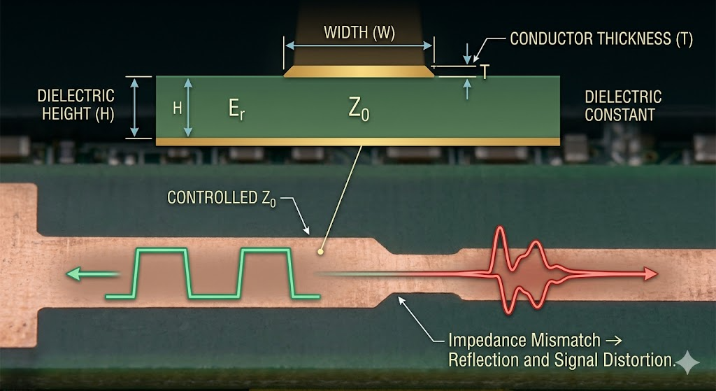
Controlled impedance is an important concept in PCB design. Each PCB trace has a characteristic impedance that is determined by the construction parameters of that trace: Width, thickness of conductor materials, dielectric materials used as well as the distance to the reference or ground plane. Impedance mismatches (discrepancies between the characteristic impedances) create reflections/echoes and signal integrity issues in the form of signal loss and/or distortion. As a result controlled PCB geometric shapes must be closely adhered to; otherwise, you will create a signal integrity and performance issue.
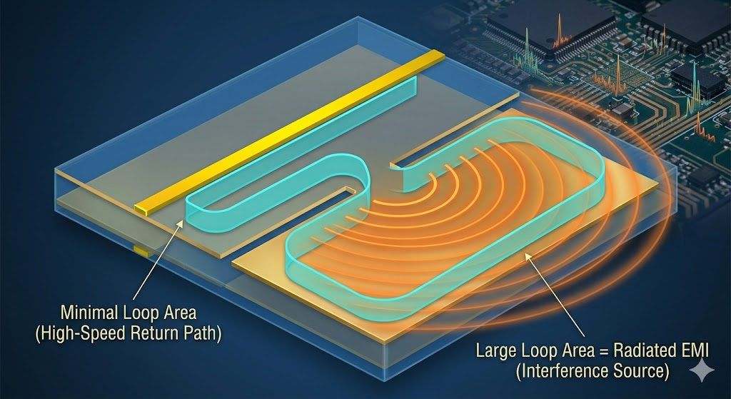
Another important concept is return path. High frequency signals will follow the path of least impedance, which will normally be directly underneath the PCB trace (on the ground plane). Any type of discontinuity (for example, split planes) will increase the loop area and cause interference problems in the forms of radiated Electro Magnetic Interference (EMI).
Material selection is important too; standard FR-4 laminate will work on many PCB applications, but as you increase frequency you have increased dielectric losses. Therefore, in high frequency applications (i.e greater than 1GHz), it is common to select lower-loss laminates to maintain signal integrity.
In addition to using proper design parameters & materials, PCB layout techniques will change when designing high frequency PCBs. Design Engineers must consider design matching of trace lengths, effects of vias (splices in traces), and parasitic types of effects. Little elements within a PCB like stubs and sharp bends can have performance ramifications. Therefore, proper routing can be vital to achieving good signal integrity.
In conclusion, the use of simulation tools and measurement tools such as field solvers and vector network analyzers (VNA’s) are an important part of validating both pre-production and post-production designs.
The bottom line for microwave PCB designs is to help control the flow of energy through the circuit as opposed to simply connecting all points. By mastering these basic components of circuit design, you will now be able to produce circuits that function reliably and with superior performance at increasingly higher frequencies.
Sign In Or Register Comment after
No comments yet. Be the first to comment!