


How to Manage Net Classes in Professional EDA Software
 View
View
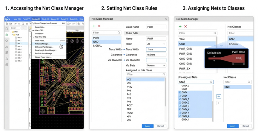
Net Classes are used to define and group specific nets together based on a common function (such as Power and/or High Speed Signals) enabling the designer to apply consistent design rules throughout the PCB layout such as Trace Width, Clearance and Layers. For example, Altium - PCB Panel > Nets > Create Net Class - allows the user to create a net class and assign all relevant nets to that particular class in order to apply rules targeted to those nets. With EasyEDA Pro, you would go to Design > Net Class Manager to create and sort your net classes and then apply them in your Design Rules. It is recommended that net classes be planned early on in the design process in any EDA tool to allow for smooth application of these design rules and to ultimately improve the manufacturability of the PCB.
Sign In Or Register Comment after
No comments yet. Be the first to comment!