


PCB Layout for Switching Regulators: Avoiding EMI Nightmares
 View
View
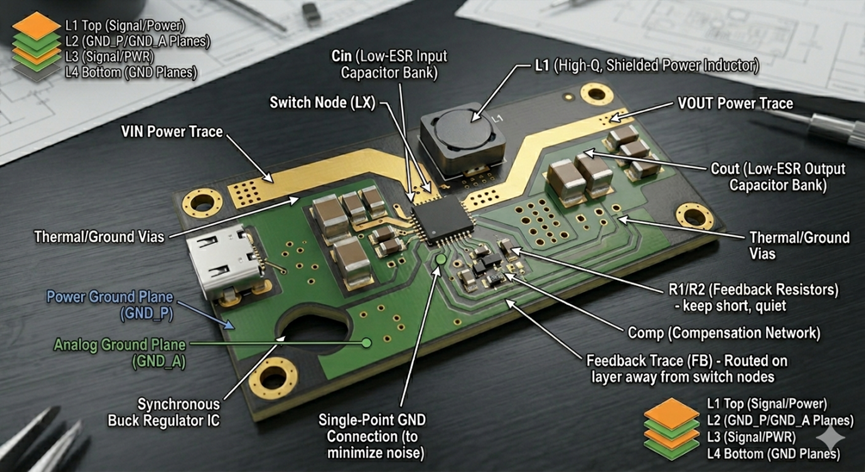
When designing your PCB layout for switching power supplies, avoid introducing an excessive amount of EMI by reducing the size of the high-current loop on your board. To accomplish this, place the power supply input/output capacitors, regulator IC, inductor, and fast recovery diode as close as possible together, because short loops produce less radiated energy/noise. Additionally, while routing your traces, use short, wide traces and a solid ground plane to create low-impedance return paths for current and reduce the inductance of the loop. Also, route sensitive signals away from the switching nodes, and keep decoupling capacitors close to their respective power pins to help suppress high frequency noise. Use these layout techniques to reduce EMI and improve reliability, performance, and compliance with applicable standards such as EMC.
#PCB#
 #PCB#
#PCB#
Sign In Or Register Comment after
No comments yet. Be the first to comment!