


How to Add Artistic Touches to Your PCB Using Silk and Copper
 View
View
Why Are PCBs so boring with their whole size being a simple rectangle that is usually a dull color? That is changing quickly! With the right imagination, your board can function as both a functional art piece and an incredibly well designed product. Nothing says, “engineer with style,” more than having a well routed ground plane on your board.
The first thing you need to think about is your silkscreen layer, which will be your canvas for logos, labels and subtle design elements. Keep your designs to a minimum (not too high a density) because a high density design will probably get clipped when it goes to manufacturing. When you do design in your silkscreen, make sure you use the right line width, which is usually greater than or equal to 0.15 mm, and don’t put a silkscreen over the pads unless you enjoy having mysterious problems when you go to solder parts onto them.
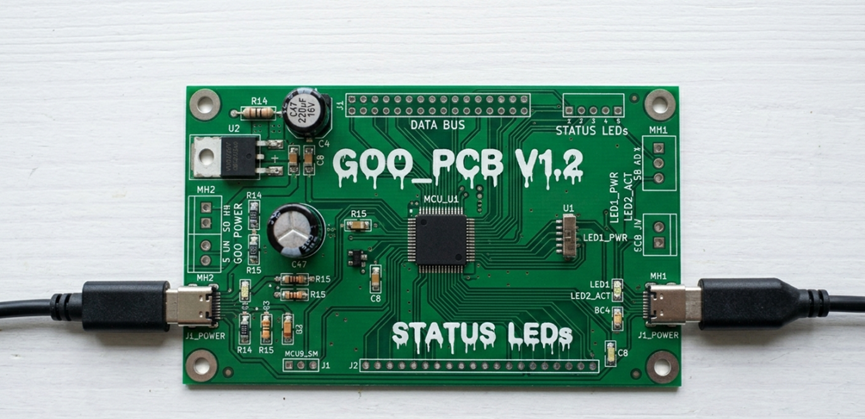
PCB silkscreen layer, Logo printing
Next, begin the process of creating your copper artwork. By designing your copper pours or traces, you can design patterns, logos, and elaborate designs directly into the board. Exposed copper (using ENIG or HASL) can look great when combined with different colors of solder mask. However, don’t forget that copper will conduct electricity, and you will not like it if you create an antenna or short to ground with your logo.
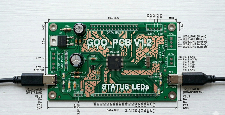
Copper pour designs on PCB
To add some additional pizzazz, try using solder mask openings to expose areas of copper that are under the solder mask. Many companies will now also have various colors of solder masks to choose from such as black, red, or blue as well as some that have a matte finish. This can give you a lot more flexibility for the aesthetics of the board.
Layer alignment is important. If the layer artwork is not aligned properly, it may appear messy. Therefore, it is critical to preview your Gerber files thoroughly. Follow the manufacturer's minimum requirements of spacing and clearance between design components, because the graphics should not negatively impact how the piece functions.
Ensure that the graphic components serve a valid purpose. The artistic portion of the layout helps improve the useability of the overall layout (via clear labels, orientation indicators, and branding), whereas the graphic components merely serve as decoratively increasing the aesthetics of the layout. By designing your PCBs properly, you can have both an attractive and functional product.
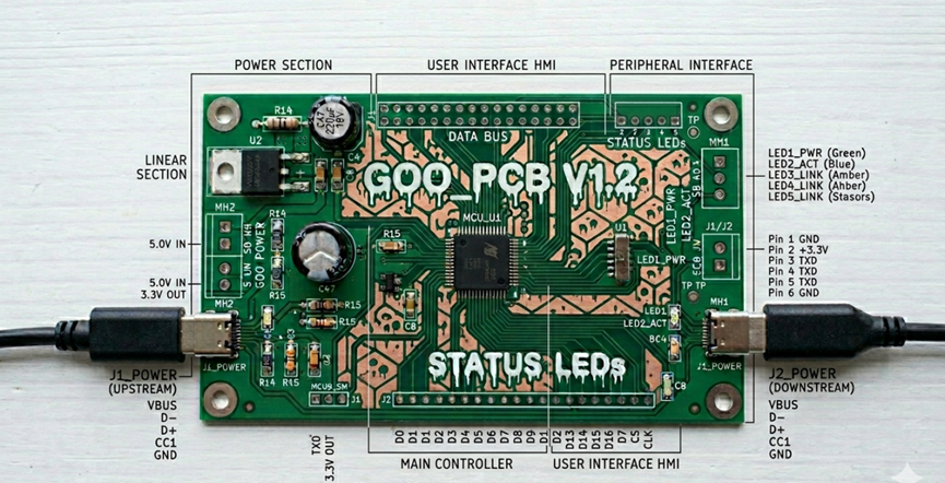
well designed PCB with proper layer alignment.
After you have completed the design process correctly (note there is a long timeline for debugging we will be doing), you will now possess a printed circuit board that functions and appears suitable for display!
Sign In Or Register Comment after
No comments yet. Be the first to comment!