


3D PCB Preview: Why You Must Check Your Clearance in 3D
 View
View
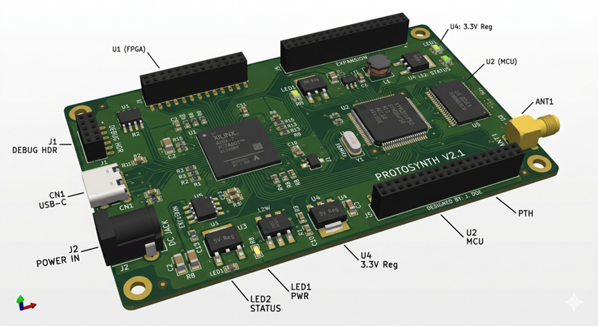
Two-dimensional layouts can be deceiving; however, the use of a three-dimensional (3D) PCB viewer in an electronic design automation (EDA) tool helps verify the heights of components as well as their alignment with connectors and fit into the housing (enclosure) prior to production. Using a 3D print model can also help in identifying other physical concerns such as possible collisions between tall components; inadequate edge clearance next to the edges; and misalignment of mechanical parts (housings/cases or heat sinks) and connections to the printed circuit board layout. Confirm all clearances for connectors, buttons, and mounting hardware. Properly routed PCBs can also fail mechanically if the 3D model has been ignored. Performing a simple 3D inspection prior to production will help eliminate expensive redesigns and assure proper fit and function of a PCB.
Sign In Or Register Comment after
No comments yet. Be the first to comment!