


Solving the "Dangling Trace" Problem: Cleaning Up Your Layout
 View
View
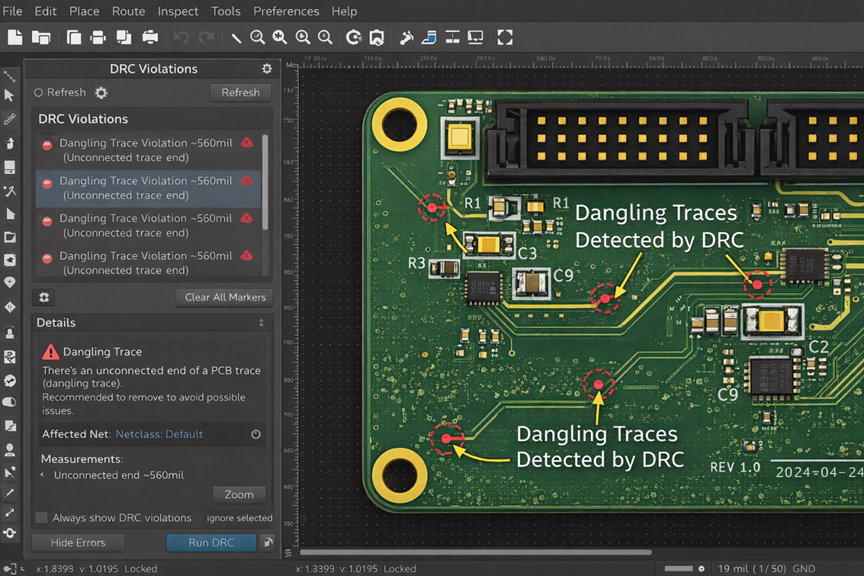
Using unconnected copper wires that have been left behind after routing changes (dangling traces) can lead to confusion, DRC errors, and unintended antennas. Run a Design Rule Check (DRC) to identify all unconnected and floating nets, and the copper that remains unconnected. Use your EDA tool’s net inspector or highlight feature to trace these unconnected and floating connections. Any floating or unused traces should be removed and/or terminated correctly, and each pad should be assured to be connected to its intended net. Having a neat layout helps to manufacture the board, reduces risk of EMI, and aids in debugging the design. A clean PCB design can look good, but also shows good engineering discipline.
PCB Design
Sign In Or Register Comment after
No comments yet. Be the first to comment!