


Ground Bounce and Power Plane Noise: Minimizing PDN Impedance
 View
View
Ground bounce may appear to be harmless; however, if a logic level has ground bounce, it will misbehave.
Ground bounce results from multiple outputs being switched off or on at the same time and then causing a current surge through the package and return paths of the PCB.
When this occurs, the ground reference at that point will temporarily move, which may lead to false switch and timing errors. In addition, power plane noise adds to the problem by causing the Power Distribution Network (PDN) to perform in a less supportive manner (i.e., as a source of instability).
The root issue is the impedance of the PDN. In other words, the impedance at high speed should not only be "low resistance" but should also be "low impedance" for all frequency ranges. Once the impedance spikes, the voltage fluctuation increases and then results in a direct noise feed into your ICs.
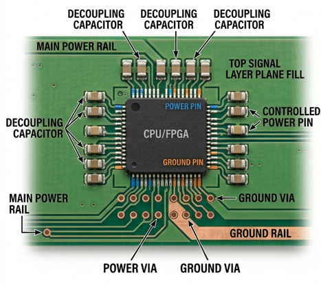
Minimizing PND impedance; PCB top view
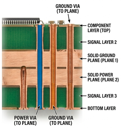
Minimizing PND impedance; PCB side view
Decoupling capacitors are the first line of defence. They should be placed as close as possible to the power pins on the device and should include at least two different values (e.g., 0.1 µF and 1.0µF) to provide decoupling for multiple frequency ranges. The small capacitors will decouple high frequency noise and the larger capacitors will provide decoupling for low frequency noise. The leads to the decoupling capacitors should be as short as possible and should use a wide trace or plane to provide a low inductance connection.
Ensure there are good, continuous power and ground planes. Avoid using splits in the power or ground planes underneath high speed signal lines, since this will interrupt the return path and increase ground bounce. Use a thin dielectric material between the power and ground planes to increase capacitance between the two, allowing for noise reduction.
Using multiple vias for power and ground connections will reduce inductive effects that can create bottlenecks. At higher frequencies, the single via will provide additional inductance that contributes to signal degradation.
Simulating your PDN prior to fabrication with specialized software will identify impedance peaks and provide proper capacitor placement as a starting point.
Ground is not a perfect ground; always treat the ground as a dynamic reference with appropriate design considerations.
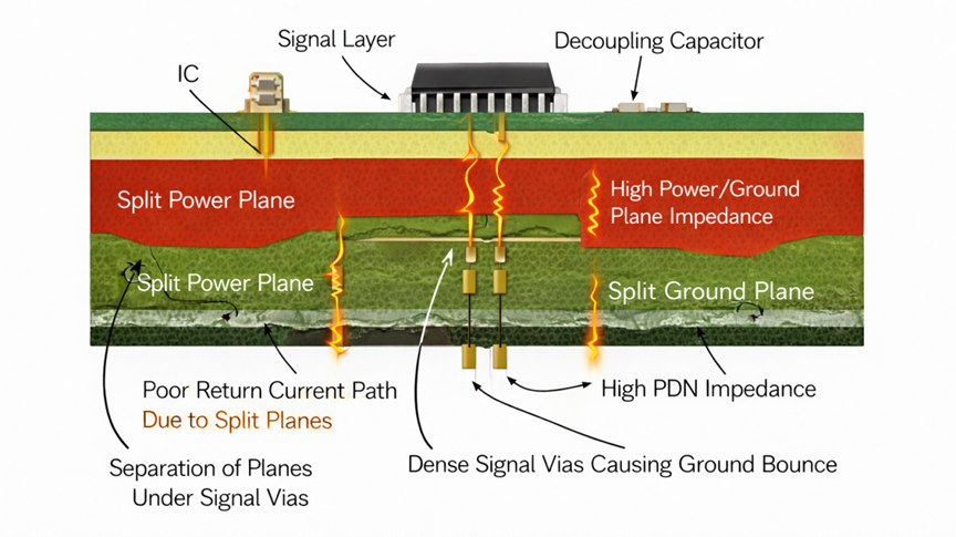
High PND impedance PCB structure
Minimizing PDN impedance is not as exciting; however, it is a necessity. Get it right, and your board will remain stable. If you get it wrong, No amount of routing will save you!
Sign In Or Register Comment after
No comments yet. Be the first to comment!