


ESP8266 Deep Dive Architecture, Memory, and GPIO Survival Guide
 View
View
ESP8266: Everything You Need to Know About the Chip That Started It All
I once had a production batch of 500 ESP8266 boards that would randomly reboot in the field, but only at night, and only in summer. Three weeks of debugging later: a slight voltage sag on the 3.3V rail combined with the ADC being read while Wi-Fi was active. The ESP8266 rewards you for understanding it deeply. This post is that understanding.
Before, we'll cover the core architecture, the notoriously tight memory layout, watchdog timers that bite the unwary, and the GPIO pins you can use without bricking your device. we'll dive into Wi-Fi operation, power management for battery life, the ADC pitfall, and when it still makes sense to design with this legendary chip.
Under the Hood: The Tensilica L106 and Why It Matters
The ESP8266 runs on a Tensilica L106 32-bit RISC core — not the most powerful architecture in the world, but one that was designed specifically for low-power, low-cost embedded applications. At 80 MHz, it handles most IoT tasks without breaking a sweat. At 160 MHz (overclock mode via system_update_cpu_freq()), it can handle some surprisingly compute-heavy tasks.
Here's the critical architecture detail that most tutorials skip: the Wi-Fi MAC layer, the TCP/IP stack, and your application code all run on this single core. Espressif manages this through a software scheduler, but the Wi-Fi stack has hard timing requirements. If your application code blocks for too long, even for 50–100 ms in some cases — you'll corrupt the Wi-Fi stack and get a reset.
This is why you'll see ESP8266 best practices always say: call yield() or delay() in any long loop. It's not optional niceness. It's the difference between a device that runs for years and one that resets every 20 minutes. The soft watchdog timer will reset the chip after exactly 3 seconds of not yielding; if disabled, the hardware WDT resets after approximately 8 seconds.
The Memory Situation (It's Tighter Than You Think)
The ESP8266 has a total of 64 KB of instruction memory (IRAM) and approximately 98 KB of DRAM space. However, the Wi-Fi stack consumes a significant portion at runtime. According to the official datasheet, when the ESP8266 is working in Station mode and connected to a router, available space in the Heap + Data sector is around 50 KB. For a simple sensor node this is fine. For anything ambitious — JSON parsing large responses, maintaining multiple network connections, running a web server with large pages — you'll hit memory walls.
IRAM (64 KB total): This is fast, tightly coupled instruction RAM. Time-critical code like ISRs and Wi-Fi callbacks runs here. You can force functions into IRAM with ICACHE_RAM_ATTR. Use this for interrupting handlers.
DRAM (~98 KB): Your heap and global variables live here. malloc(), String objects, global arrays, they all eat into this pool. Monitor your free heap with ESP.getFreeHeap() and ESP.getHeapFragmentation().
External Flash (SPI): Firmware, SPIFFS/LittleFS, RF calibration data. Typically 1–16 MB. The flash is connected via SPI at 40 or 80 MHz. Code runs from cache, but large functions that don't fit in cache cause flash reads — which can cause issues during Wi-Fi TX. Non-cached code runs 12–13 times slower than code from IRAM; cached code runs as fast as from IRAM.
Monitor your heap during development. Call Serial.println(ESP.getFreeHeap()) after major operations. If it trends downward over time, you have a memory leak — most likely a String object or buffer not being freed.
GPIOs: Which Ones Are Actually Safe to Use
The ESP8266 has 17 GPIO pins, but several of them are landmines for the uninitiated. The chip has boot mode strapping pins that must be in specific states during power-on. Get this wrong and your device either won't boot or won't enter flash mode.
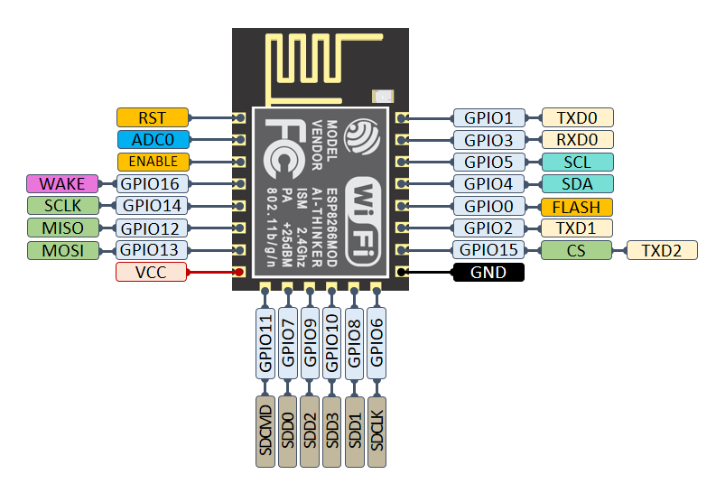
| Label | GPIO | Input | Output | Notes |
|---|---|---|---|---|
| D0 | GPIO16 | no interrupt | no PWM or I2C support | HIGH at boot; used to wake up from deep sleep |
| D1 | GPIO5 | OK | OK | often used as SCL (I2C) |
| D2 | GPIO4 | OK | OK | often used as SDA (I2C) |
| D3 | GPIO0 | pulled up | OK | connected to FLASH button, boot fails if pulled LOW |
| D4 | GPIO2 | pulled up | OK | HIGH at boot; connected to on-board LED, boot fails if pulled LOW |
| D5 | GPIO14 | OK | OK | SPI (SCLK) |
| D6 | GPIO12 | OK | OK | SPI (MISO) |
| D7 | GPIO13 | OK | OK | SPI (MOSI) |
| D8 | GPIO15 | pulled to GND | OK | SPI (CS); boot fails if pulled HIGH |
| RX | GPIO3 | OK | RX pin | HIGH at boot |
| TX | GPIO1 | TX pin | OK | HIGH at boot; debug output at boot, boot fails if pulled LOW |
| A0 | ADC0 | Analog Input | X | 0–1V analog input only |
⚠️ GPIO6–GPIO11 are connected to the internal SPI flash bus. Never attempt to use them. You will crash the chip. This catches people who look at the package pinout and think they have more GPIOs available than they do.
Sign In Or Register Comment after
No comments yet. Be the first to comment!