


I Thought the PCB Was Ready Until DRC Disagreed
 View
View
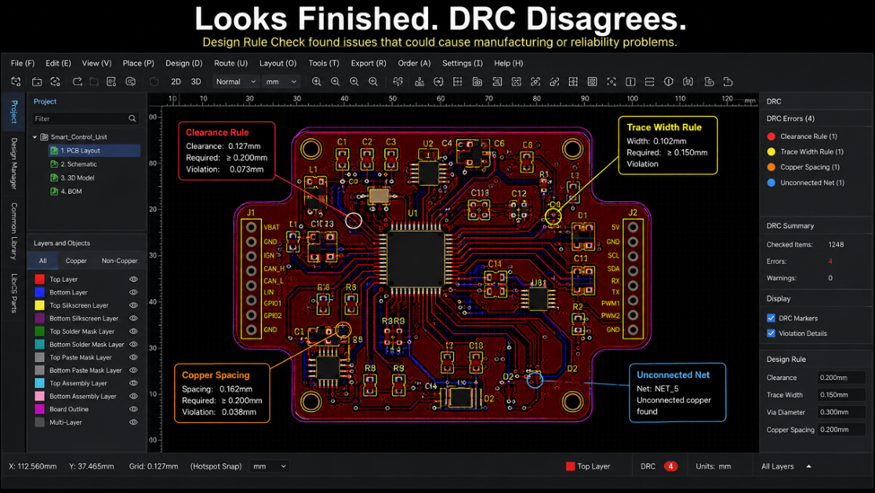
There have been times when a PCB looked finished.
The routing was done, the placement looked clean, and nothing seemed out of place.
Then I ran DRC.
Sometimes it was a clearance issue I hadn't noticed. Sometimes it was a trace width rule, a copper spacing violation, or another constraint that looked acceptable visually but didn't match the design rules.
That's one reason I don't rely only on what I see on the screen.
A PCB can look finished and still violate the rules it was designed to follow.
Before generating manufacturing files, I always let DRC have the final opinion.
#JLCPCB# #EasyEDA# #PCBLayout# #DRC# #PCBDesign# #Electronics#
 #JLCPCB#
#EasyEDA#
#PCBLayout#
#DRC#
#PCBDesign#
#Electronics#
#JLCPCB#
#EasyEDA#
#PCBLayout#
#DRC#
#PCBDesign#
#Electronics#
Layout
Sign In Or Register Comment after
No comments yet. Be the first to comment!