


The PCB Didn't Change; The Gerber View Did
 View
View
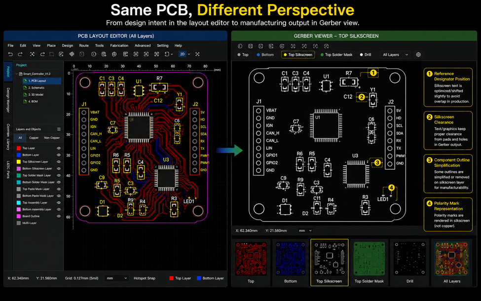
One habit I've developed before placing an order is opening the Gerber Viewer, even when I'm confident the PCB layout is complete.
The PCB itself hasn't changed, but viewing the manufacturing files gives me a different perspective. Copper layers, silkscreen, solder mask openings, and drill holes are shown exactly as they will be produced.
Most of the time, everything looks fine.
Occasionally, I notice a silkscreen label that's too close to a pad, a copper pour that doesn't look as expected, or another small detail that I overlooked while editing the layout.
It's a simple check that gives me extra confidence before sending the board for manufacturing.
#JLCPCB# #EasyEDA# #Gerber# #PCBLayout# #PCBDesign# #Electronics#
 #JLCPCB#
#EasyEDA#
#Gerber#
#PCBLayout#
#PCBDesign#
#Electronics#
#JLCPCB#
#EasyEDA#
#Gerber#
#PCBLayout#
#PCBDesign#
#Electronics#
Layout
Sign In Or Register Comment after
No comments yet. Be the first to comment!