


A Busy PCB Is Easier to Review One Net at a Time
 View
View
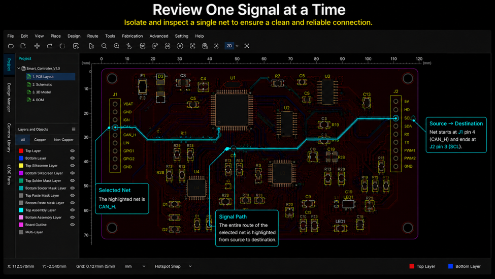
As a PCB layout becomes denser, reviewing signal paths by eye becomes increasingly difficult. Traces overlap visually, copper pours fill empty spaces, and it's easy to lose track of a single connection among hundreds of others.
Highlighting one net simplifies the review process. Instead of scanning the entire board, the focus stays on a single signal from its source to its destination. This makes it much easier to confirm the route, check unnecessary detours, and understand how that signal travels across the board.
It isn't intended to replace DRC or electrical verification. It's simply another way to review routing from a different perspective before generating the manufacturing files.
#JLCPCB# #EasyEDA# #PCBLayout# #SignalRouting# #PCBDesign# #Electronics#
 #JLCPCB#
#EasyEDA#
#PCBLayout#
#SignalRouting#
#PCBDesign#
#Electronics#
#JLCPCB#
#EasyEDA#
#PCBLayout#
#SignalRouting#
#PCBDesign#
#Electronics#
Sign In Or Register Comment after
No comments yet. Be the first to comment!