


Why Differential Pair Spacing Matters More Than You Think
 View
View
When engineers first start learning about high-speed PCB design, the discussion often revolves around length matching. While matching the lengths of a differential pair is important, it's only part of what makes the routing perform well. One detail that's often underestimated is maintaining consistent spacing between the two traces.
For interfaces such as USB, Ethernet, LVDS, CAN FD, or PCIe, differential pairs are designed to carry equal and opposite signals. As these signals travel together, they create electromagnetic fields that couple with each other. This coupling is one of the reasons differentials signaling offers better noise immunity and lower EMI than single-ended routing.
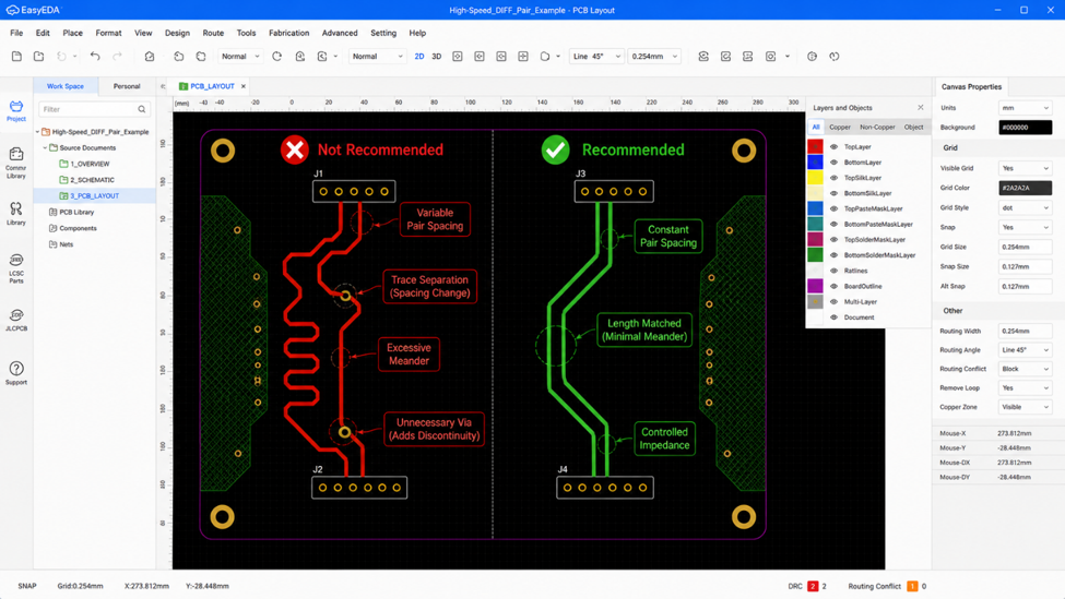
Although spacing may only change by a fraction of a millimeter, its effect can be significant in high-speed circuits. Every change in spacing modifies the coupling between the traces, which directly affects the differential impedance. Instead of behaving as one transmission structure, the pair begins to behave differently along different sections of the route.
This doesn't necessarily mean the PCB will fail immediately, but it reduces the design margin and makes signal integrity more difficult to predict, especially as data rates continue to increase.
Good differential pair routing therefore focuses on maintaining a consistent geometry rather than simply producing equal trace lengths.
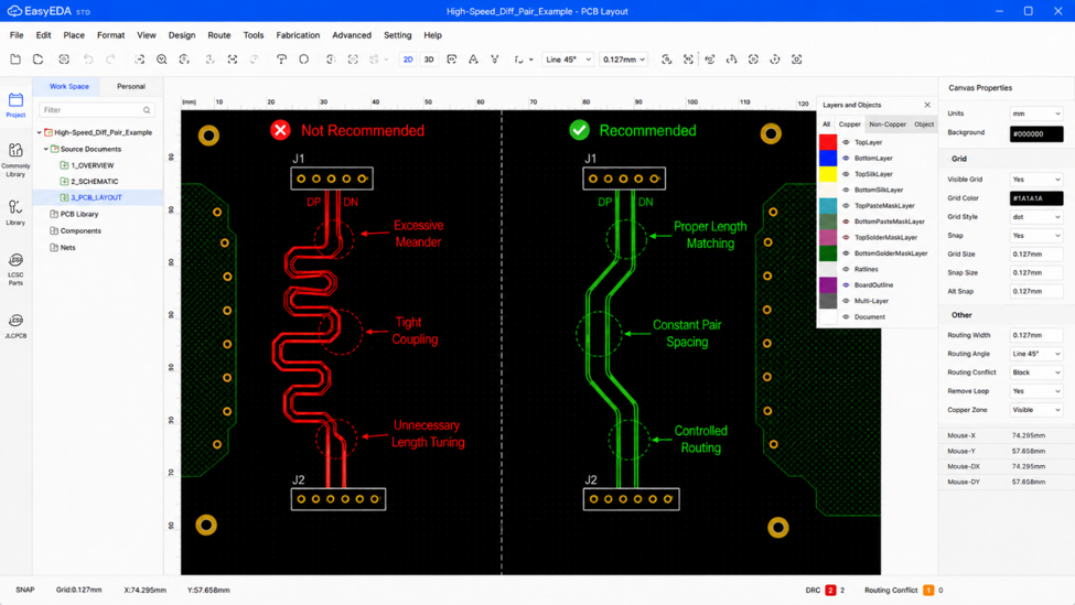
During PCB layout, maintaining constant spacing is not always easy. Connectors, BGAs, vias, and mechanical constraints often force designers to adjust routing. Modern PCB software provides differential pair routing tools to help preserve width and spacing automatically, but engineering review is still essential.
Another common misconception is that adding more serpentine routing automatically improves length matching. Excessive meanders placed too closely together may increase intra-pair coupling and create additional signal integrity issues. Length tuning should only be applied where necessary and should follow the recommendations provided by the PCB manufacturer or signal integrity requirements.
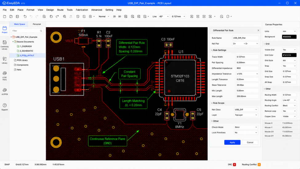
One habit that has helped me during PCB reviews is to stop looking only at trace length. Instead, I review the differential pair as a single transmission path. I check whether both traces remain together, whether their spacing changes unexpectedly, and whether they stay referenced to the same continuous ground plane.
These small reviews only take a few minutes but often catch routing issues before the design reaches manufacturing.
Differential pair routing is not just about making two traces reach the destination at the same time. Consistent spacing, controlled impedance, and a continuous reference plane all contribute to maintaining signal integrity. By treating the pair as a single transmission structure rather than two independent traces, engineers can build more reliable high-speed PCB designs with fewer surprises during testing and production.
#JLCPCB# #EasyEDA# #PCBLayout# #DifferentialPair# #HighSpeedPCB# #SignalIntegrity#
 #JLCPCB#
#EasyEDA#
#PCBLayout#
#DifferentialPair#
#HighSpeedPCB#
#SignalIntegrity#
#JLCPCB#
#EasyEDA#
#PCBLayout#
#DifferentialPair#
#HighSpeedPCB#
#SignalIntegrity#
Sign In Or Register Comment after
No comments yet. Be the first to comment!