


Why Clock and Reset Signals Deserve Extra Protection
 View
View
Not every signal on a PCB requires the same level of routing attention. While many digital signals can tolerate small routing imperfections, clock and reset lines often play a much more critical role in overall system stability.
A noisy clock signal may introduce timing uncertainty, while an unstable reset line can lead to unexpected resets or unreliable startup behavior. These issues are often difficult to reproduce because they depend on switching activity, electromagnetic interference, and the PCB layout itself.
For this reason, experienced PCB designers usually give clock and reset nets a higher routing priority than ordinary digital signals.
Why Clock and Reset Signals Are Different
Clock signals provide timing reference for processors, microcontrollers, memory devices, and communication peripherals. Every rising and falling edge must arrive with minimal distortion and predictable timing.
Reset signals may switch only occasionally, but they are extremely sensitive during power-up and system initialization. Noise coupled into a reset line can unintentionally reset the processor or prevent the system from starting correctly.
Because both signals influence the entire system rather than a single peripheral, their routing deserves additional protection.
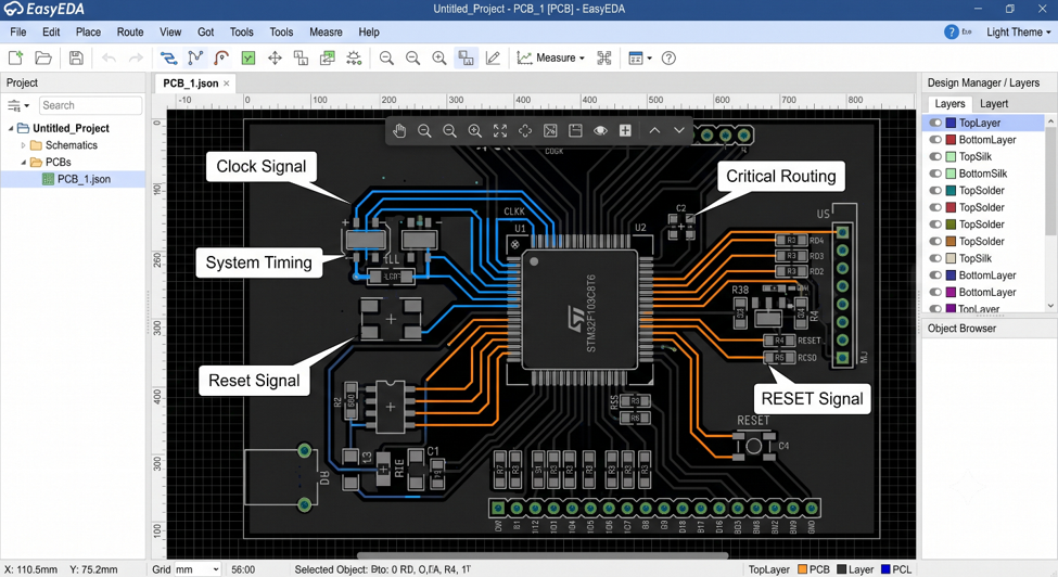
Common Design Mistakes
One common mistake is routing clock and reset signals alongside noisy switching circuits or parallel to high-current traces for long distances.
Another issue is leaving these signals completely exposed without any consideration for nearby interference sources.
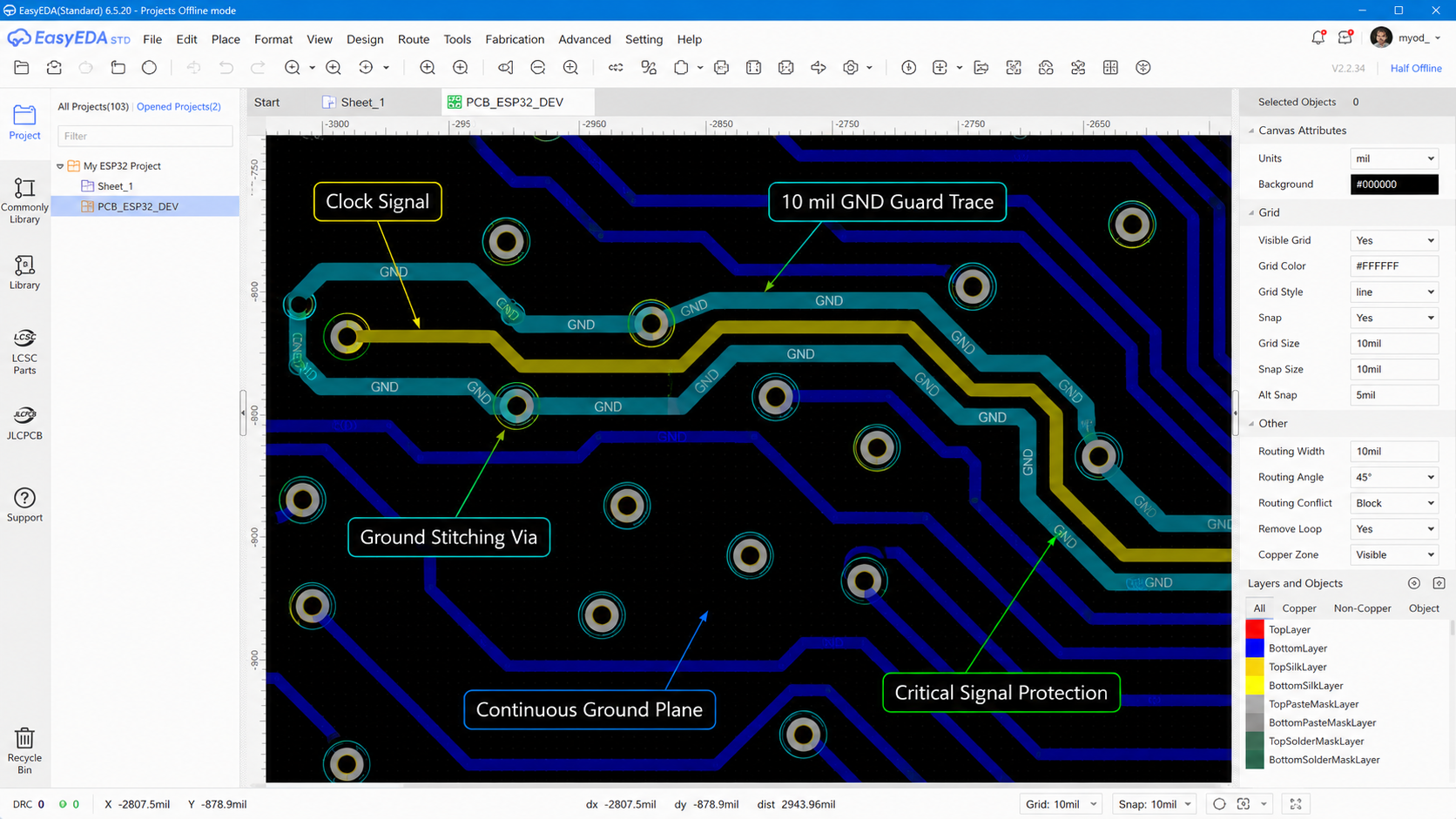
The Pattern Design Guide recommends enclosing clock signals with a grounded guard trace or ground shape. It also recommends protecting critical signals such as CLK and RESET using approximately 10 mil GND guard traces where appropriate.
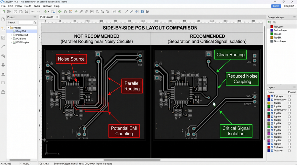
Recommended Design Practice
One practical technique used in many designs is surrounding critical signals with grounded guard traces or adjacent ground copper connected through stitching vias.
The guard trace does not eliminate every source of interference, but it helps reduce electromagnetic coupling from nearby switching activity. Combined with a continuous reference plane and careful component placement, this creates a cleaner routing environment for critical timing signals.
As always, the final routing should follow the reference layout recommended by the component manufacturer whenever one is provided.
Design Review Checklist
Before releasing the PCB for manufacturing, I review every critical timing signal using a few simple questions.
- Is the clock routed through a quiet area?
- Is the reset line separated from noisy power circuits?
- Does the routing remain above a continuous reference plane?
- Is a ground guard implemented where recommended?
- Does the layout follow the device reference design?
These checks only take a few minutes but often prevent difficult debugging work after assembly.
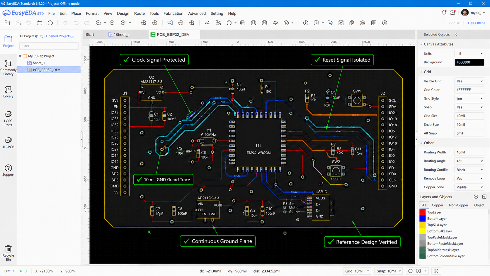
Clock and reset signals occupy only a small portion of most PCB layouts, yet they influence the stability of the entire system. Giving these nets extra routing attention, protecting them from nearby noise, and following the reference design can significantly improve system reliability without adding much complexity to the PCB.
#JLCPCB# #EasyEDA# #PCBLayout# #ClockSignal# #SignalIntegrity# #HighSpeedPCB#
 #JLCPCB#
#EasyEDA#
#PCBLayout#
#ClockSignal#
#SignalIntegrity#
#HighSpeedPCB#
#JLCPCB#
#EasyEDA#
#PCBLayout#
#ClockSignal#
#SignalIntegrity#
#HighSpeedPCB#
Sign In Or Register Comment after
No comments yet. Be the first to comment!