


How to Route Differential Pairs on a PCB
 View
View
Differential signaling is used in USB, HDMI, Ethernet, LVDS, and many other high-speed protocols because it rejects common-mode noise far better than single-ended traces. Getting it right on a PCB means more than placing two traces side by side.
Impedance Target
Both traces in a differential pair must have the same length and the same impedance. A mismatch converts differential signal to common-mode noise, causing jitter and bit errors. Common targets:
• USB 2.0: 90Ω differential
• USB 3.0 / LVDS: 100Ω differential
• Ethernet: 100Ω differential
Your PCB manufacturer's stackup calculator gives you the trace width and spacing to hit the target. JLCPCB offers controlled-impedance manufacturing with ±10% tolerance, specify it at the order stage.
Routing Rules
Practical rules for differential pairs:
• Route both traces simultaneously — use the differential pair mode in EasyEDA, KiCad, or Altium
• Keep traces tightly coupled: spacing within 3–5× trace width for the full length
• Match trace lengths: skew must stay under one unit interval (UI). For USB 2.0 at 480Mbps that is roughly 14mm
• If vias are necessary, place them on both traces at the same location
• Never route a differential pair over a split or gap in the reference plane
• Maintain at least 3× trace width clearance to adjacent single-ended nets
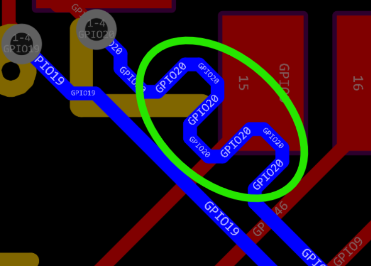
Matched-length pair with serpentine length compensation
Length Matching
Use serpentine meanders to compensate for length skew within a pair. Keep meander amplitude under 3× trace width to avoid adding excess parasitic inductance. Place meanders close to where the skew originates, not all bunched at the end of the route. Most EDA tools have a built-in length-matching tool that handles this automatically.
Sign In Or Register Comment after
No comments yet. Be the first to comment!