


6 Layer PCB Stackup: What It Is and When to Use It
 View
View
6-layer PCB cross-section showing layer arrangement
A 4-layer board often is not enough when a design mixes dense routing, high-speed signals, and distributed power nets. A 6-layer board gives you two extra routing layers, dedicated power and ground planes, and better EMI shielding, at a modest cost increase over 4-layer.
Standard Stackup
The most common 6-layer arrangement:
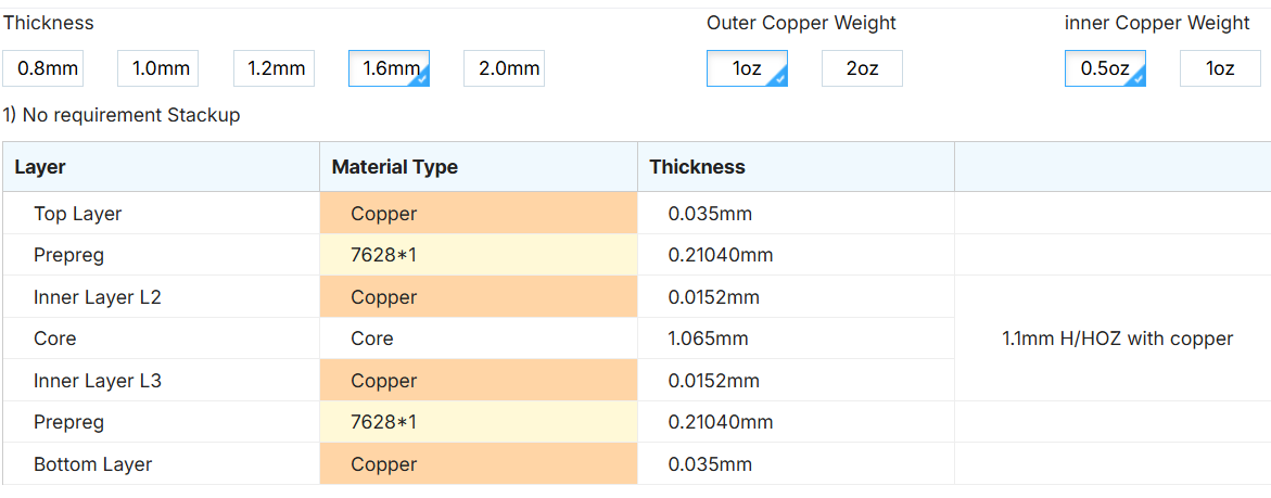
• L1 (Top): Signal + components
• L2: Ground plane
• L3: Signal (inner)
• L4: Power plane
• L5: Ground plane
• L6 (Bottom): Signal + components
L1 and L6 each sit directly next to a ground plane, giving every surface trace a clean, unbroken return path. L3 is sandwiched between L2 (ground) and L4 (power), shielded on both sides. Which makes it ideal for high-speed differential pairs or sensitive analog signals.
Design Guidelines
Tips for 6-layer board design:
• Route high-speed signals on L1, L6, or L3, all three have adjacent reference planes
• Use L4 as a partial power pour, not a full flood, full flooding between L4 and L5 can create parallel-plane resonance at high frequency
• Never route across a split in the reference plane on any layer, return current will detour and radiate
• If mixing high-speed digital and switching power on the same board, separate ground pours and stitch them at a single point near the input connector
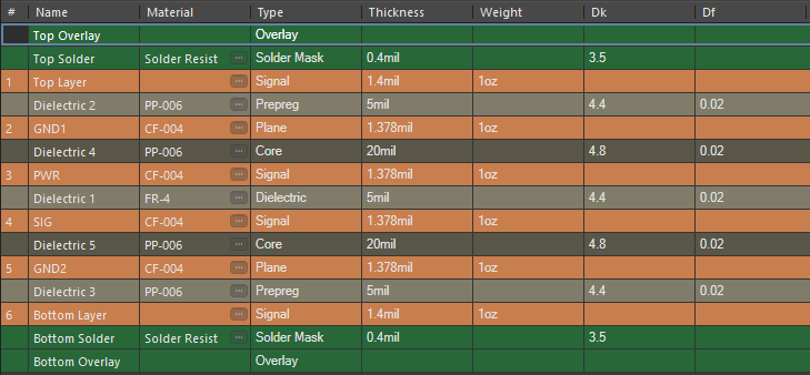
Dielectric layer arrangement and typical thickness values
Via Considerations
Through-hole vias on a 6-layer board traverse all six layers even if only connecting L1 to L3. The unused stub adds capacitance and degrades signal quality above 1GHz. Options to fix it:
• Blind vias (e.g. L1–L2 only) remove the stub entirely for HDI routing
• Back-drilled vias eliminate the stub on through-hole vias for critical nets
JLCPCB supports blind, buried, and back-drilled vias, check their capabilities page for minimum drill sizes and allowed layer combinations before routing.
Sign In Or Register Comment after
No comments yet. Be the first to comment!