


Design for Assembly (DFA): Small Design Choices That Make PCB Assembly Easier
 View
View
A PCB that passes electrical testing is not always easy to assemble. During product development, engineers often focus on schematic accuracy and PCB routing while overlooking how the board will be populated during manufacturing.
This is where Design for Assembly (DFA) becomes important. DFA is the practice of designing a product so that components can be assembled more easily, consistently, and with fewer manufacturing errors.
Simple decisions such as component orientation, spacing, and connector placement can reduce assembly time, improve inspection, and increase production yield.
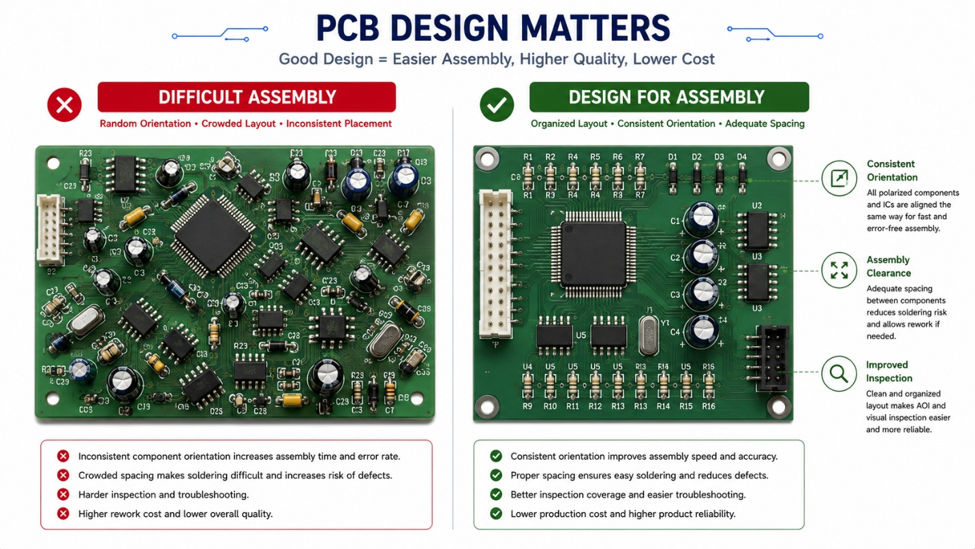
Why Component Orientation Matters
Although modern pick-and-place machines can place components in almost any orientation, consistent placement still provides important benefits.
For example:
- Polarized capacitors facing the same direction are easier to inspect.
- IC pin 1 markers become easier to verify.
- Connectors with consistent orientation simplify cable assembly.
- Manual rework becomes faster and less error prone.
These improvements are especially valuable during prototype assembly and production debugging.
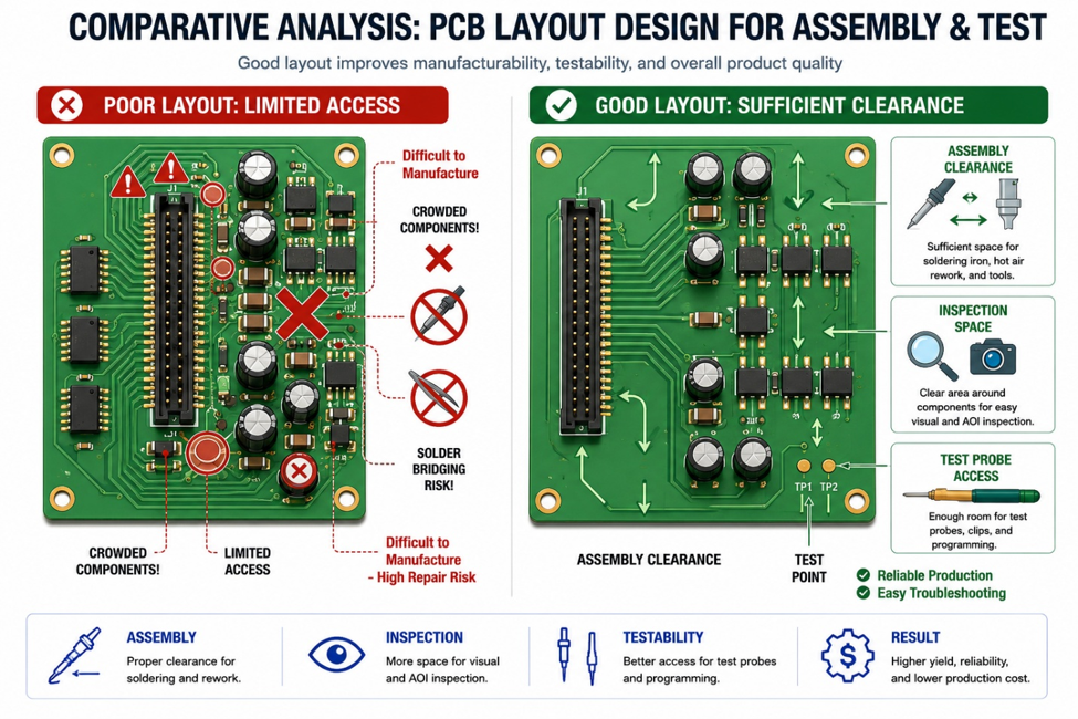
Leave Enough Working Space
Components placed too close together may complicate soldering, inspection, and future repairs.
Provide adequate spacing around:
- Connectors
- Test points
- Large electrolytic capacitors
- Heat-generating components
Good spacing also improves accessibility for probes during functional testing.
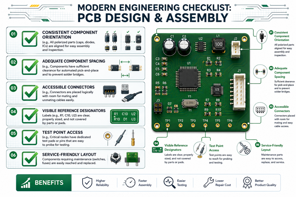
Practical DFA Checklist
Before releasing a PCB for manufacturing, review:
- Are polarized components oriented consistently?
- Are connectors accessible after assembly?
- Is there enough clearance for soldering and inspection?
- Can test probes reach important measurement points?
- Are reference designators visible after components are installed?
These simple checks take only a few minutes but can prevent unnecessary production issues.
Engineering Tip
A PCB should not only be easy to manufacture but also be easy to assemble, inspect, test, and repair. Considering these stages during layout often saves far more time than optimizing a few millimeters of routing.
Design for Assembly is about making manufacturing more efficient through better design decisions. By paying attention to component orientation, spacing, accessibility, and inspection, engineers can reduce production problems and improve overall product quality.
Good PCB design is not finished when routing is complete—it is finished when the board can be assembled reliably and efficiently.
#DesignAndManufacturing# #PCBAssembly# #DFA# #PCBDesign# #ElectronicsManufacturing# #Engineering#
 #DesignAndManufacturing#
#PCBAssembly#
#DFA#
#PCBDesign#
#ElectronicsManufacturing#
#Engineering#
#DesignAndManufacturing#
#PCBAssembly#
#DFA#
#PCBDesign#
#ElectronicsManufacturing#
#Engineering#
Sign In Or Register Comment after
No comments yet. Be the first to comment!