


Keeping Components Away from PCB Edges
 View
View
When designing a PCB, it's tempting to use every available millimeter of board space. Components are often placed as close as possible to the edges to keep the layout compact.
However, placing components too close to the board edge can create unexpected problems during manufacturing, assembly, and even everyday use. A little extra clearance can help improve both the reliability and durability of the finished product.
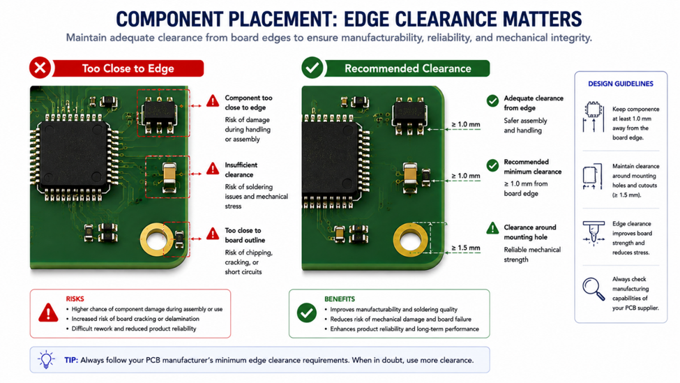
Why Edge Clearance Matters
The edges of a PCB experience more mechanical stress than many designers realize.
During depaneling, installation, or routine handling, the board can flex slightly. If sensitive components are located too close to the edge, they may be exposed to unnecessary mechanical stress.
This is especially important for ceramic capacitors, connectors, and other components that can be affected by bending forces.
Components That Deserve Extra Space
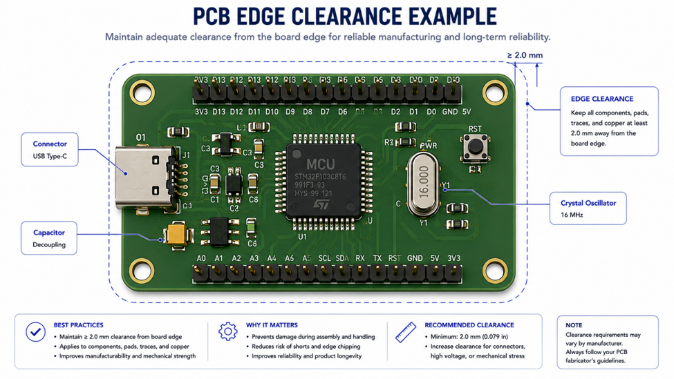
While every design is different, it's usually a good idea to leave additional clearance for components such as:
- USB connectors
- Pin headers
- Ceramic capacitors
- Large inductors
- Crystal oscillators
- Tall components near mounting points
Giving these parts a little more room helps reduce the chance of mechanical damage during assembly and long-term use.
Think Beyond the PCB Layout
Edge clearance isn't only about manufacturing.
Consider how the finished product will be used. Will users frequently plug and unplug cables? Will the PCB be mounted inside an enclosure? Will screws apply pressure near the corners?
Thinking about these real-world conditions during the design stage often leads to a more reliable product.
Engineering Tip
Before sending your PCB for manufacturing, take one final look around the board outline. If any component appears too close to the edge, consider whether a little extra clearance could improve reliability without affecting the overall design.
Making full use of the available PCB area may seem efficient, but leaving appropriate clearance around the board edges is often a better long-term design choice. A small amount of extra space can help reduce mechanical stress, simplify assembly, and improve the overall durability of the finished PCB.
Good PCB design is not only about fitting components it is also about ensuring they remain reliable throughout the product's lifetime.
#DesignAndManufacturing# #PCBDesign# #PCBLayout# #HardwareDesign# #Electronics# #PCB#
 #DesignAndManufacturing#
#PCBDesign#
#PCBLayout#
#HardwareDesign#
#Electronics#
#PCB#
#DesignAndManufacturing#
#PCBDesign#
#PCBLayout#
#HardwareDesign#
#Electronics#
#PCB#
Sign In Or Register Comment after
No comments yet. Be the first to comment!