


 View
View
Full article on JLCPCB: https://jlcpcb.com/blog/logic-gate-symbols-guide
The same NAND gate appears as a bubbled D-shape in one schematic and a rectangle marked & in the next. Neither is wrong. ANSI/IEEE Std 91-1984 defines both families, so calling the rectangle the non-ANSI form is a review comment worth dropping. What actually flips your output is the bubble.
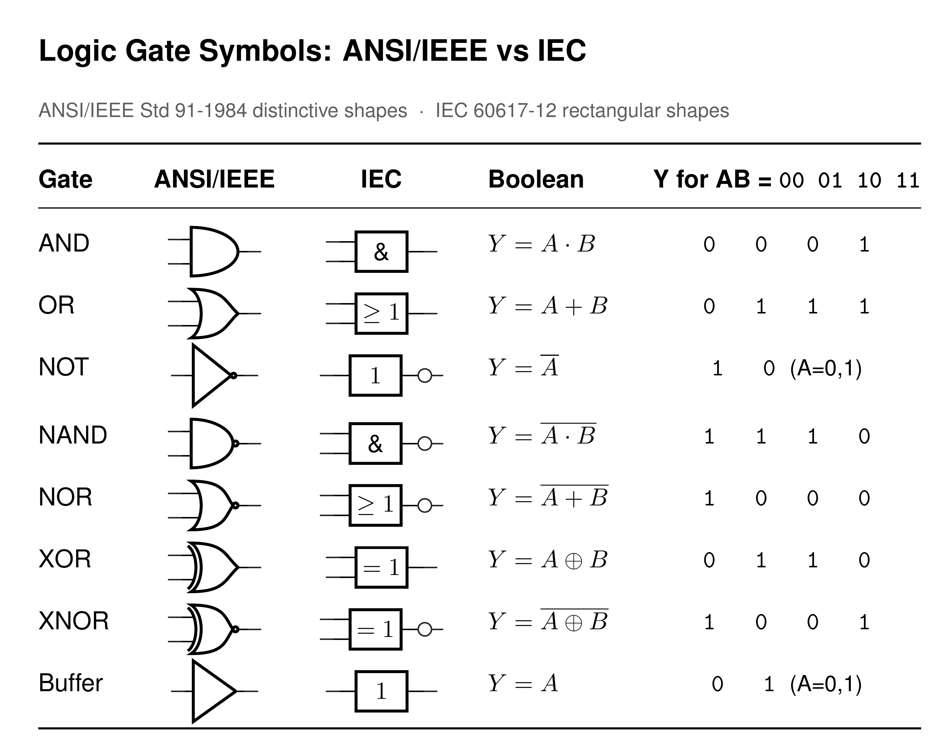
Every logic gate in ANSI distinctive shape and IEC rectangular form, side by side
Two Symbol Sets
The distinctive shapes came from MIL-STD-806 in the early 1960s and passed into ANSI/IEEE Std 91-1984. IEC 60617-12 standardised the rectangle, which names the function with a qualifying symbol printed inside it rather than by outline. Pick one set per drawing set, and never mix both on a sheet: a reviewer scanning for shapes will skip a rectangle.
· AND: flat back, curved nose. IEC qualifier &
· OR: curved back, pointed nose. IEC qualifier at least 1
· XOR: OR shape, doubled input line. IEC qualifier =1
· NOT and buffer: triangle, with and without the bubble. IEC qualifier 1
· NAND, NOR, XNOR: the same outlines with an output bubble
· Rail range decides the family: 74HC runs 2 V to 6 V, 4000B runs 3 V to 18 V
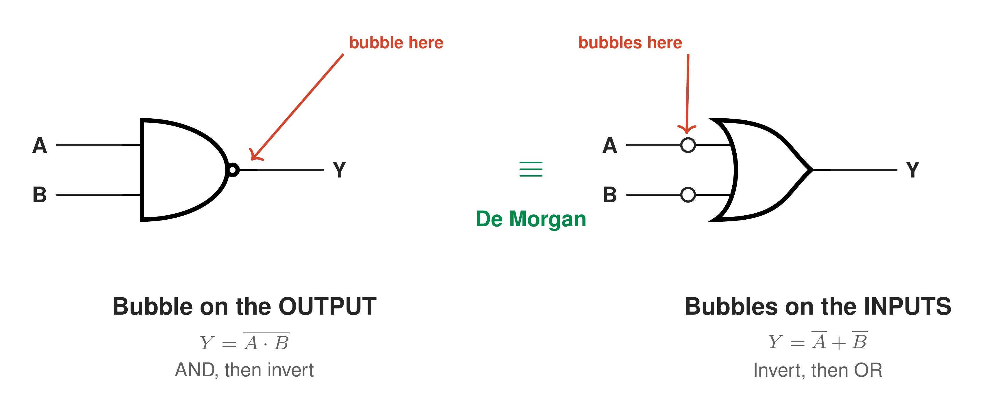
Inversion bubble anatomy, output bubble compared with input bubbles on the same gate
Reading The Bubble
The small circle is a negation indicator, not decoration. On an output it complements the function, so AND becomes NAND and OR becomes NOR. On an input it marks that pin active LOW, and the gate sees the inverted net. An OR shape with bubbles on both inputs is the same gate as a NAND, because (A · B)' = A' + B'. That De Morgan equivalent is drawn deliberately, so the bubbles line up with active-low net names such as nCS or /OE. A wedge instead of a circle marks an active-low pin without inverting the function.
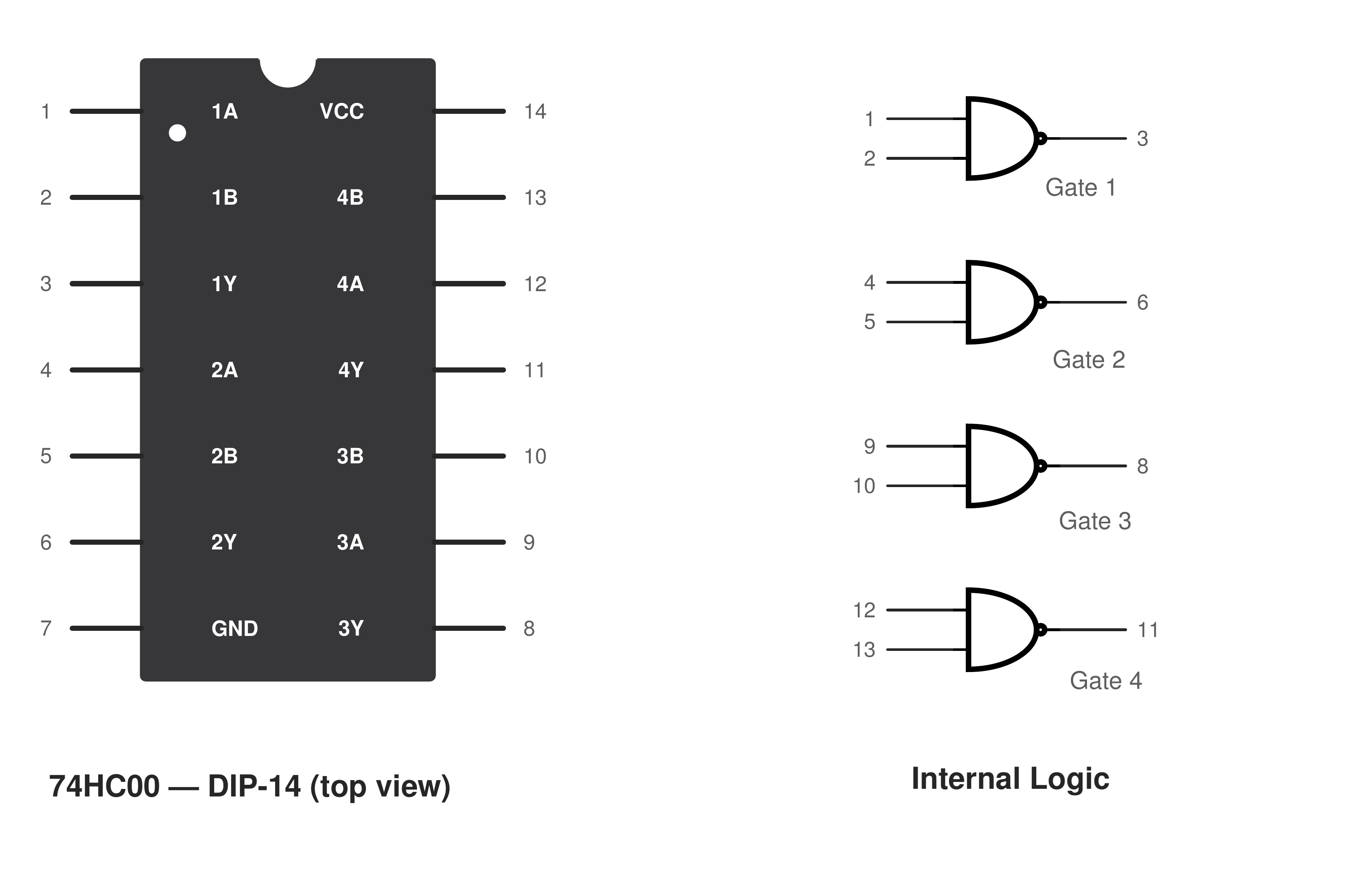
74HC00 quad 2-input NAND pinout, 14-pin package
Symbol To Package
One symbol is rarely one part. A 74HC00 quad NAND is U1A to U1D on the schematic and a single SOIC-14 on the layout, sharing one VCC pin and one decoupling capacitor. Tie every unused CMOS input to VCC or GND, because a floating input self-biases, oscillates and raises supply current. Do not assume pin compatibility either: the 74HC02 places its outputs on pins 1, 4, 10 and 13, so it cannot share a 74HC00 footprint.
The full ANSI and IEC chart, all eight truth tables, the NAND-only gate counts and the 74xx to 4000-series part lookup are in the complete guide: Read the full guide
Sign In Or Register Comment after
No comments yet. Be the first to comment!