


Power Supply Symbols, Circles and Diamonds
 View
View
Full article on JLCPCB: https://jlcpcb.com/blog/power-supply-symbols-ultimate-guide
A circle, a diamond, and three shrinking horizontal bars. Three power supply symbols, three different meanings, and only one of them is an independent source. Draw a controlled source as a circle and your simulation settles on a completely wrong operating point. Neither that error nor an implicit chassis-to-earth tie trips a design rule check.
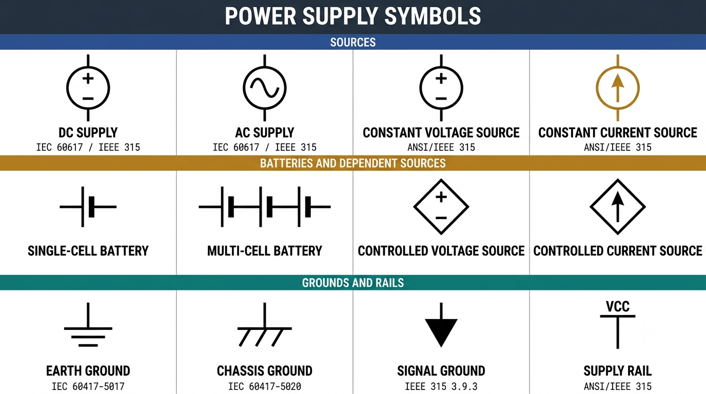
The power supply symbol chart: DC, AC, source, battery and ground symbols side by side
Four Symbol Families
Fourteen symbols cover almost every power source you will meet on a schematic, and they sort into four families: sources, batteries, grounds and rail labels. The outline answers the first question before you read a single label.
· Circle: independent source. Polarity marks for DC, a sine wave for AC, an arrow for current
· Diamond: dependent source, output set by another circuit quantity
· Unequal bar pairs: battery. The long thin bar is positive, one pair per cell
· Earth ground: three shrinking bars, IEC 60417-5017, IEEE 315 clause 3.9.1
· Chassis ground: one bar with three angled strokes, IEC 60417-5020, clause 3.9.2
· Signal ground: downward triangle, IEEE 315 clause 3.9.3
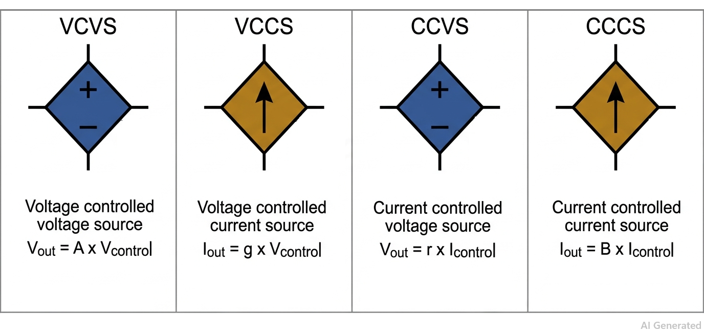
The four dependent source symbols drawn as diamonds with their controlling variables
Why A Diamond
The diamond outline is the only visual difference between a controlled source and an independent one. VCVS and CCVS carry polarity marks; VCCS and CCCS carry an arrow. This is how every active device is modelled: a bipolar transistor is a CCCS, a MOSFET is a VCCS, an ideal op-amp is a VCVS, and a current-sense amplifier behaves as a CCVS. One caveat. The diamond is a drafting convention, not a numbered entry in IEC 60617 the way the earth mark is numbered in IEC 60417, so treat it as binding practice but never cite a clause number for it.
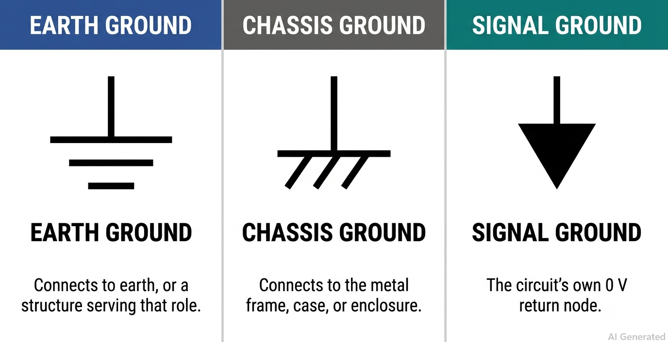
Earth, chassis and signal ground symbols drawn at equal scale for comparison
Three Grounds
Earth, chassis and signal ground are three separate nets. IEEE 315 clause 3.9.2 notes explicitly that a chassis may sit at a substantial potential relative to the earth around it, so placing both glyphs on one net without an explicit bond creates a ground loop that shows up as a failed EMC scan rather than a DRC error. AGND, DGND and PGND all reuse the signal ground triangle, and only the label changes. That is what lets a layout tool keep three returns apart and join them at one defined tie point. If you cannot find that tie point, the schematic has a defect.
The full 14-symbol chart, the IEC 60617 versus ANSI/IEEE 315 comparison, the four dependent source equations and the symbol-to-footprint table are in the complete guide: Read the full guide
Sign In Or Register Comment after
No comments yet. Be the first to comment!