


 View
Hi makers!
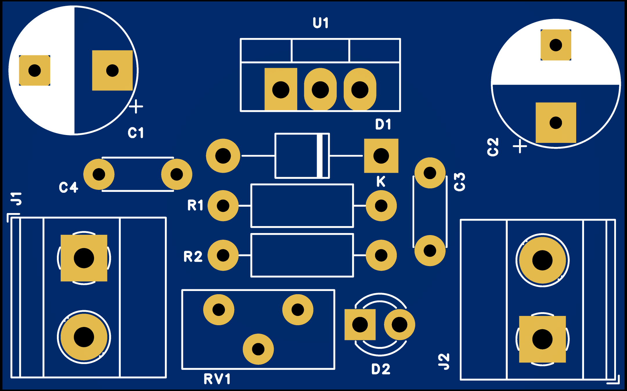
This schematic represents an Adjustable Linear Voltage Regulator (Power Supply) circuit. Its primary purpose is to take a higher, DC input voltage and convert it into a lower, stable, and adjustable DC output voltage.
Before sending a PCB off for manufacturing, I prefer to experiment using either a breadboard or a test board. In this case, however, experimenting on a breadboard is easy. After that, an order is placed with JLCPCB.
1. Core Component: LM1084-ADJ
The heart of the circuit is the U1 LM1084-ADJ.
Function: It is a Low Dropout (LDO) positive voltage regulator.
Capacity: The LM1084 is capable of handling high currents (up to 5 Amps with a serious heatsink), making this a robust power supply compared to standard regulators like the LM317 (which handles 1.5A).
2. Input Stage
• J1 (9-20V): This is the input connector. It accepts a DC voltage between 9 Volts and 20 Volts.
• C1 (330uF) & C3 (100nF): These are input capacitors.
• C1 is a large bulk capacitor that smooths out low-frequency ripples from the power source.
• C3 is a small ceramic capacitor that filters out high-frequency noise and prevents the regulator from oscillating.
3. Voltage Adjustment
This is how the output voltage is controlled:
• R1 (120R): This resistor is connected between the Output and the Adjust pin. It sets the reference current. A value of 120Ω is standard for these regulators to ensure a minimum load current (approx. 10mA) so the regulator stays stable.
• RV1 (5k Potentiometer): This is a variable resistor connected to the Adjust pin. By turning this knob, you change the resistance, which changes the output voltage.
The Formula: The output voltage is determined by the formula: Vout=1.25V×(1+RV1R1)V_{out} = 1.25V \times (1 + \frac{RV1}{R1})Vout=1.25V×(1+R1RV1).
With a 120Ω fixed resistor and a 5k variable resistor, the theoretical range is roughly 1.25V to ~53V.
However, since the input is max 20V, the output can never exceed the input (minus a small "dropout" voltage of ~1.5V). So the practical max output is around 18V. The label 3.3-16V on J2 indicates the intended safe operating range.
4. Protection Diode (Top)
D1 (1N4007): This diode is a protection component. It is connected in reverse bias (Cathode to Input, Anode to Output).
Function: If the input power is suddenly disconnected or shorted to ground, the large capacitors on the output side (C2) would try to discharge back through the regulator, which could destroy it. D1 provides a safe path for this current to flow back to the input side, protecting the LM1084 chip.
5. Output Stage
• C4 (100nF) & C2 (100uF): These are output capacitors. They improve the transient response (how fast the regulator reacts to load changes) and ensure the output voltage is smooth and stable.
• R2 (1k) & D2 (LED): This is a simple indicator circuit. When the output voltage is present, current flows through the resistor and lights up the LED, indicating the power supply is active.
• J2 (3.3-16V): This is the output connector where you would connect your load (the device you are powering).
This description was created partly using A.I.
Most of the time I use salvaged components or buy from local store, but I tried to build a BoM for you too using LCSC.com supplier.
The project is presented as is, made for hobby projects.



Enjoy it! 🤓
#PCB# #LM1084#
 #PCB#
#LM1084#
Sign In Or Register Comment after
No comments yet. Be the first to comment!