Why Your ADC Readings Keep Jumping Even When Nothing Changes

You're monitoring a sensor with a microcontroller, but something doesn't seem right. The measured value constantly changes by a few counts even though the sensor is perfect still. You check the software, replace the sensor, and even recalibrate the system, yet the readings continue to fluctuate.

This behavior is one of the most common challenges in embedded system design. In many cases, the ADC itself isn't faulty the surrounding hardware is simply introducing noise into the measurement.

Understanding where ADC noise comes from is the first step toward building more stable and accurate measurement systems.

image.png

Common Sources of ADC Noise

Although ADC resolution is often specified in bits, measurement quality depends heavily on the surrounding hardware.

Some of the most common causes of unstable ADC readings include:

  • Long analog signals act as antennas.
  • Switching noise from nearby DC-DC converters.
  • Poor grounding between analog and digital circuits.
  • Missing decoupling capacitors.
  • High-impedance sensor outputs driving the ADC directly.

Each of these factors introduces small voltage variations that the ADC faithfully converts into changing digital values.

image.png

Engineering Note

Increasing ADC resolution does not automatically improve measurement accuracy. If the analog input is noisy, a 16-bit ADC may simply provide a more detailed measurement of the noise.

Practical Ways to Improve ADC Stability

Reliable ADC measurements usually result from several small improvements rather than one major change.

A simple RC low-pass filter can attenuate high-frequency noise before the ADC input. Keeping analog traces short reduces electromagnetic pickup, while placing decoupling capacitors close to the microcontroller helps stabilize the supply voltage. Using a continuous ground plane and separating noisy switching circuits from sensitive analog inputs also improves measurement consistency.

For software, averaging multiple samples or applying a moving-average filter can further reduce random fluctuations without requiring hardware modifications.

image.png

Recommended Components

Several common components help improve analog signal quality before the ADC.

Component Typical Value Typical Application
Murata GRM188R71H104KA93 100 nF Supply decoupling
Yageo RC0402FR-0710KL 10 kΩ RC input filter
Murata GRM188R60J105KA01 1 µF Analog input filtering
Texas Instruments OPA320 Rail-to-Rail Op-Amp Buffering high-impedance sensors

Always refer to the ADC input characteristics in the microcontroller datasheet, especially the recommended source impedance and sampling time.

An unstable ADC reading is rarely caused by the converter itself. More often, the problem originates from power supply noise, poor PCB layout, grounding issues, or inadequate signal conditioning. By treating the analog signal path as carefully as the digital circuit, engineers can achieve measurements that are both accurate and repeatable.

#AnalogAndSignal# #ADC# #SignalConditioning# #EmbeddedSystems# #Microcontroller# #Electronics#

Analog & Signal
Why Open-Drain Outputs Need Pull-up Resistors

When a digital output changes state, most engineers expect it to actively drive the signal either HIGH or LOW. This is true for push-pull outputs, which are commonly used on microcontrollers. However, not every digital output works this way.

Many integrated circuits, sensors, and communication interfaces use open-drain outputs instead. Unlike push-pull outputs, an open-drain pin can only pull the signal LOW. It cannot drive the line HIGH by itself.

Without a pull-up resistor, the output simply remains floating when the transistor turns off. This often leads to unstable logic levels and communication failures, especially for engineers encountering open-drain circuits for the first time.

Understanding why pull-up resistors are required helps explain how buses such as I²C allow multiple devices to share the same communication lines safely.

image.png

Why Open-Drain Exists

Although push-pull outputs are faster, open-drain outputs provide an important advantage: multiple devices can safely share the same signal line.

The line remains in a HIGH state via the pull-up resistor as long as no device actively pulls it down. Once any device forces the line LOW, the whole bus drops to LOW safely, eliminating the risk of conflicting outputs.

This principle is widely used in I²C communication, interrupt lines, reset circuits, and wired-AND logic.

Engineering Note

If two push-pull outputs accidentally drive opposite logic levels at the same time, excessive current can flow between the devices. Open-drain outputs avoid this problem by allowing devices to pull the line LOW only.

Choosing the Right Pull-up Resistor

The value of the pull-up resistor affects both power consumption and signal rise time.

A resistor that is too large causes slow rising edges, especially on buses with high capacitance. A resistor that is too small increases current consumption whenever the line is pulled LOW.

For many embedded applications, values between 2.2 kΩ and 10 kΩ are commonly used, with 4.7 kΩ being one of the most popular choices for standard I²C buses.

image.png

Recommended Devices

Open-drain outputs are commonly found in many digital ICs and communication devices.

Device Output Type Typical Applications
PCF8574 Open-Drain I²C GPIO Expander
MCP23017 Open-Drain Interrupt Output GPIO Expansion
BME280 Open-Drain I²C Interface Environmental Sensor
AT24C256 Open-Drain I²C Interface EEPROM Memory

Always consult the device datasheet to determine whether external pull-up resistors are required, as some development boards already include them on the PCB.

Open-drain output may seem unusual at first because they cannot generate a HIGH level on their own. However, this simple architecture enables multiple devices to safely share a communication line, making it ideal for buses such as I²C and other shared digital interfaces. Understanding how pull-up resistors work with open-drain output helps engineers design more reliable embedded systems.

#EmbeddedSystems# #OpenDrain# #I2C# #PullUpResistor# #Microcontroller# #Electronics#

Embedded Systems2
Not Every Capacitor Belongs Next to the Power Input

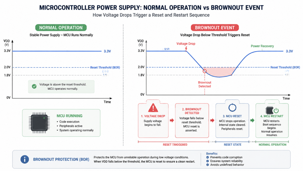
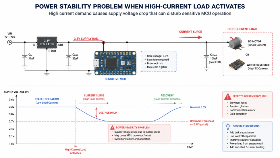
Capacitors are among the most common components in electronic circuits, yet their placement is just as important as their value. Many beginners focus on selecting the correct capacitance while the exact location on the PCB makes little difference. Moving a capacitor only a few centimeters away from where it is needed can significantly reduce its effectiveness.

This is especially true for power supply filtering. Different capacitors serve different purposes, and understanding where each one should be placed helps improve power stability, reduce noise, and prevent unexpected system behavior.

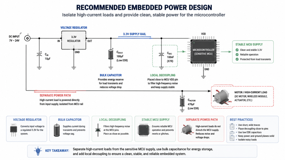
Rather than placing every capacitor near the power connector, good designs distribute capacitors according to the electrical demands of the circuit.

image.png

Understanding Their Different Roles

A bulk capacitor, typically an electrolytic or polymer capacitor, acts as an energy reservoir. It helps smooth low-frequency voltage ripple and supplies current during larger load changes. For this reason, it is usually placed close to the power connector or voltage regulator.

A decoupling capacitor serves a different purpose. Small ceramic capacitors, such as 100 nF, respond much faster to rapid current demands generated by microcontrollers, digital ICs, and communication devices. They should be positioned as close as possible to each power pin to minimize trace inductance.

Although both improve power quality, they work together rather than replacing one another.

image.png

Engineering Note

A 100 nF capacitor located 30 mm away from a microcontroller is often far less effective than one placed only a few millimeters from the VCC pin. At high frequencies, trace inductance can become more significant than the capacitor value itself.

Practical Design Tips

When reviewing a PCB layout, don't simply count the number of capacitors. Instead, verify that each capacitor is positioned according to its function.

A practical rule is:

  • Place bulk capacitors near the power entry or voltage regulator.
  • Place 100 nF ceramic capacitors immediately beside every MCU or digital IC power pin.
  • Use wider power traces and a continuous ground plane to reduce impedance.
  • Keep the connection between the capacitor and the IC as short as possible.

These simple placement practices often improve power integrity without changing the circuit schematic.

image.png

Recommended Components

The following capacitors are commonly used together in embedded and digital power systems.

Component Typical Value Typical Applications
Murata GRM188R71H104KA93 100 nF Ceramic MCU and digital IC decoupling
Samsung CL10B104KB8NNNC 100 nF Ceramic General-purpose bypass capacitor
Panasonic FR Series 47–220 µF Electrolytic Power input filtering
Nichicon UHE Series 100–470 µF Electrolytic Bulk energy storage

Always refer to the microcontroller or IC datasheet, as many manufacturers specify the recommended capacitor values and placement guidelines for optimal performance.

Choosing the correct capacitor value is only part of good circuit design. Proper placement determines how effectively that capacitor can perform its job. By placing bulk capacitors where power enters the circuit and locating decoupling capacitors directly beside each IC, engineers can significantly improve power stability, reduce electrical noise, and build more reliable electronic systems.

#PowerAndEnergy# #DecouplingCapacitor# #PowerIntegrity# #PCBDesign# #EmbeddedSystems# #Electronics#

Power & Engery