Electronic Community JLCDMP Mechanical Community OSHWLab JLCPCB JLC3DP JLCCNC JLCMC JLCONE EasyEDA JLCCAN LCSC Cable LCSC Panel




Everything looks fine on paper — until testing starts. 🤔
🛠️ For CNC machined parts, effective shielding often begins much earlier than the enclosure stage. Material choice, surface finish, and grounding design all play a role in how interference is controlled.
Small design decisions at the part level can make a big difference in overall EMI/RFI performance. 🔍
📘 Here’s a practical overview of common EMI/RFI shielding approaches for CNC machined parts — and how engineers decide between them 👇
https://jlccnc.com/blog/emi-rfi-shielding-for-cnc-machined-parts




Hi all,
The question is about this schematic and the correct order of the Zener diode and caps from the power supply to VBAT.
In SIM800C&R800C Compatible Design we have:

Also, SIM800C_Hardware_Design_V1.05 says "The correct flow from source to VBAT pin should go though Zener diode then huge capacitor;" on pg 39 which matches the above circuit
But the schematic on easyeda.com puts the zener diode close to the VBAT instead of the power supply.
Shouldn't I use that circuit for the SIM? Am rather confused.
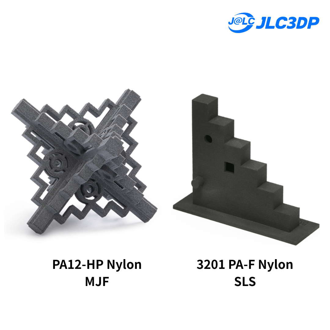
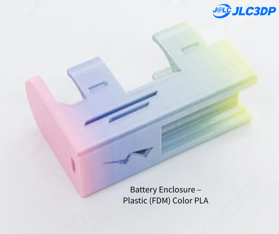
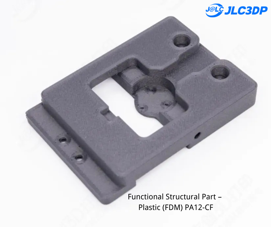
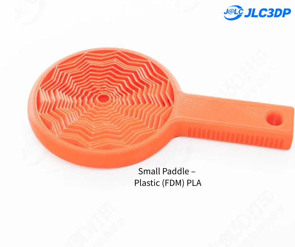
Durable structural parts.
Rock-solid enclosures.
Flexible, functional details.
Engineering plastic 3D prints hide way more clever design than you might expect.
No long talk—just scroll and feel the texture 👇
From concept models to real-world functional parts, engineering plastics make ideas usable.
👉 All these materials are now available on https://jlc3dp.com?from=socialmedia
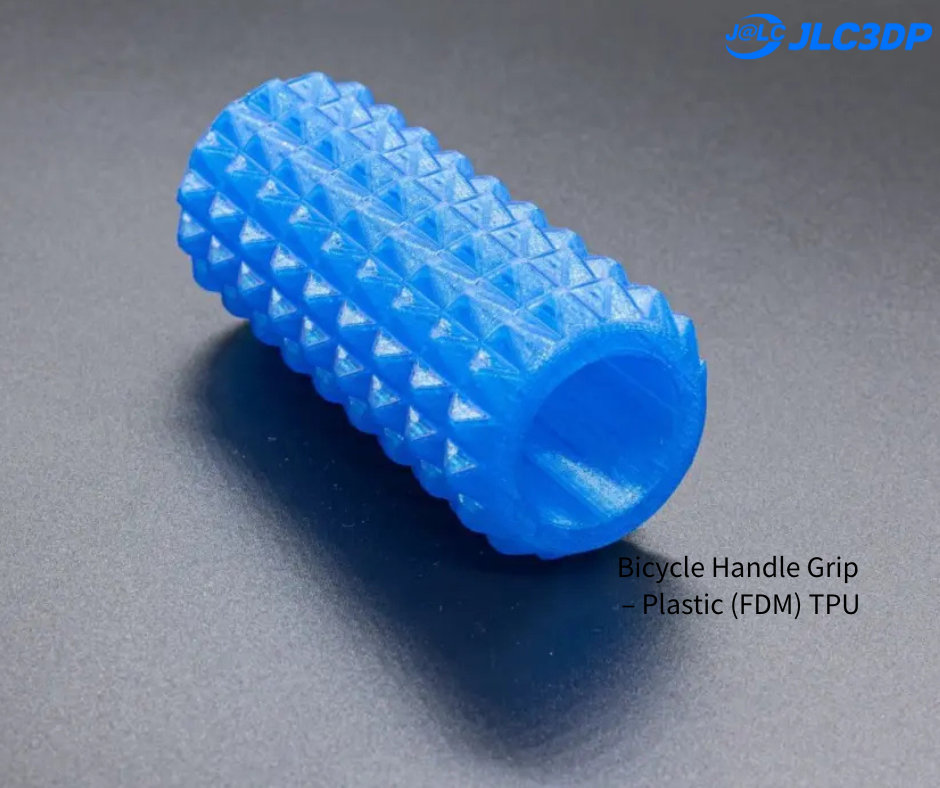

They start by solving a real problem.
If you’ve used 3D printing to:
• fix something
• improve a design
• build a functional part
• or finish a real project
We’d love to see it.
The JLC3DP Creator Spotlight is currently open — featuring real-world 3D printing projects from engineers and makers.
What you get:
• Featured on JLC3DP’s Customer Cases page
• Up to $100 in coupons + kit gift set
• $15 no-minimum coupon just for sharing
📅 Ongoing until Mar 15 (GMT+8)
Just post your project, tag @JLC3DP, and use #JLC3DPSpotlight.
👉 Full details here:
https://jlc3dp.com/blog/jlc3dp-creator-spotlight-3d-printing-contest
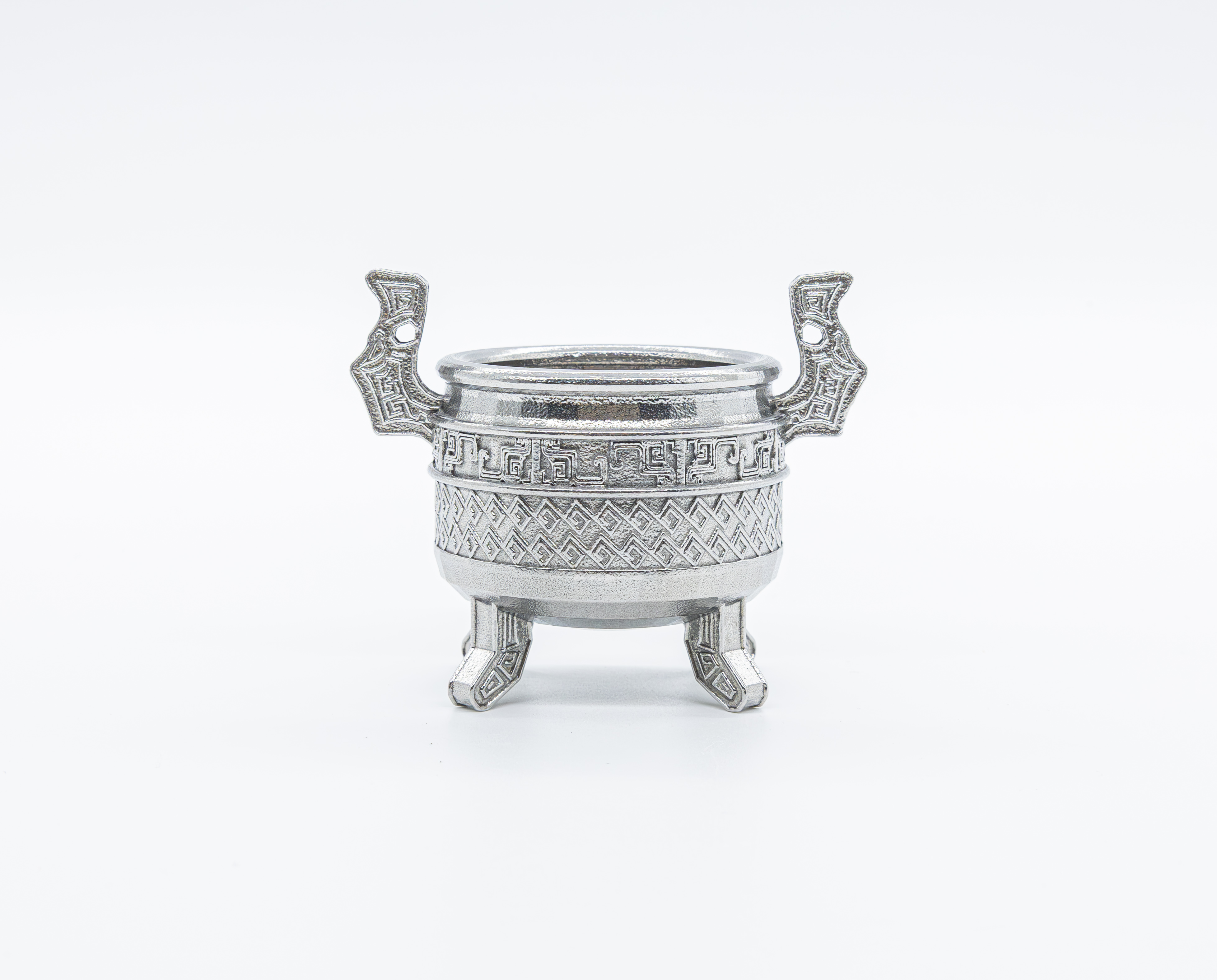
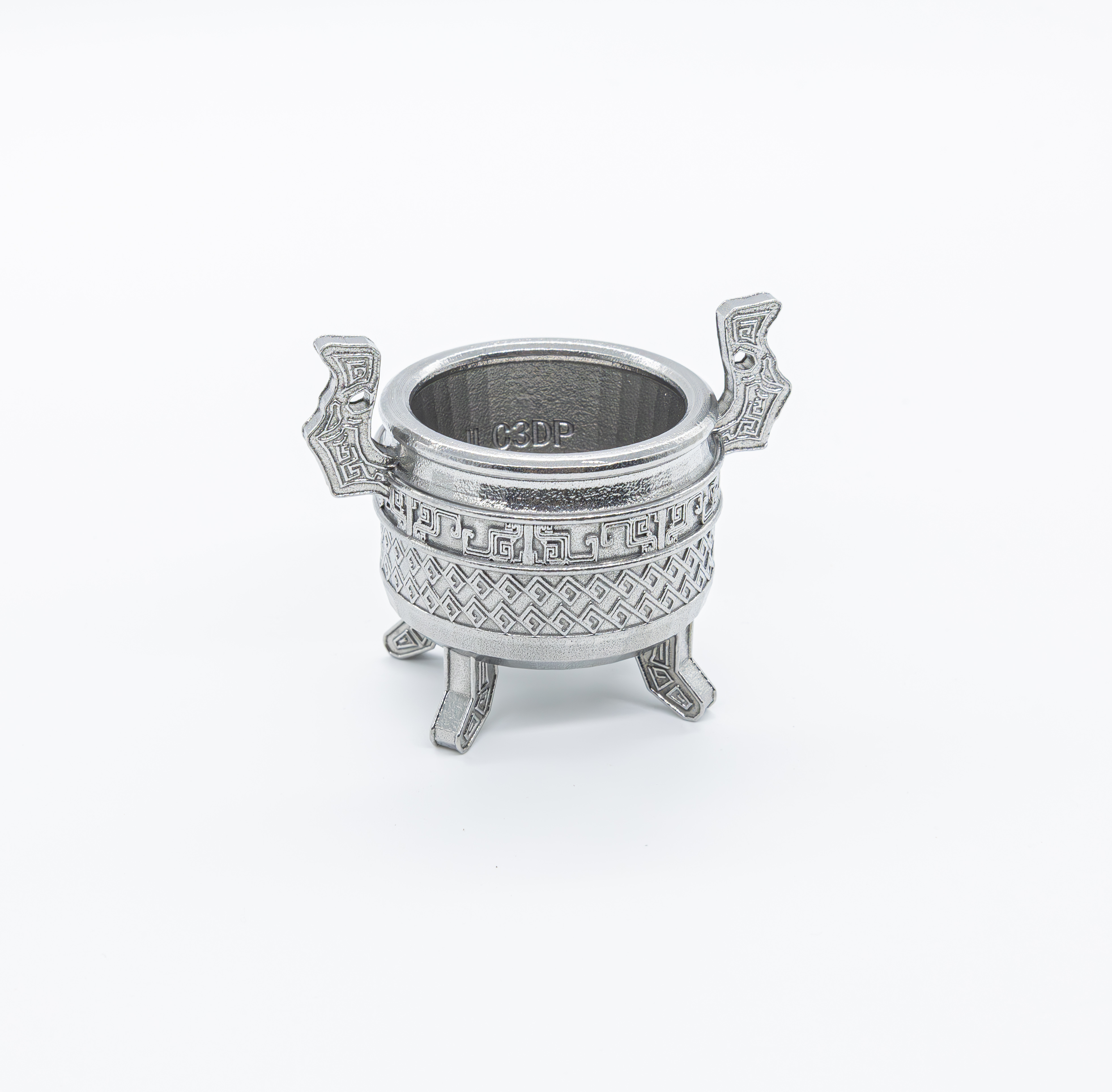

Here’s a recent hands-on case we loved:
a palm-sized ancient-style bronze ding, made entirely with metal 3D printing. 👇
Not cast.
Not CNC-machined.
Printed using Binder Jetting (BJ) with 316L stainless steel.
Why this worked surprisingly well:
• Binder Jetting + BJ-316L → captures fine ornamental lines with sharp edges
• Consistent detail at curves & corners → no blur, no broken patterns
• Standard polishing post-process → even surface gloss, solid hand feel
• Engravable surface → supports text & secondary detailing
When traditional motifs meet modern additive manufacturing,
even a small object gets an entirely new way of being made.
💰 Why makers care:
BJ metal printing lowers both cost and lead time compared to traditional metal forming — without sacrificing surface detail.
🎁 Limited-time offer:
BJ-316L metal printing now comes with up to $47 in coupons
👉 Try it here: https://jlc3dp.com/coupon-center?from=BJC
What kind of traditional or decorative geometry would you try with metal 3D printing?
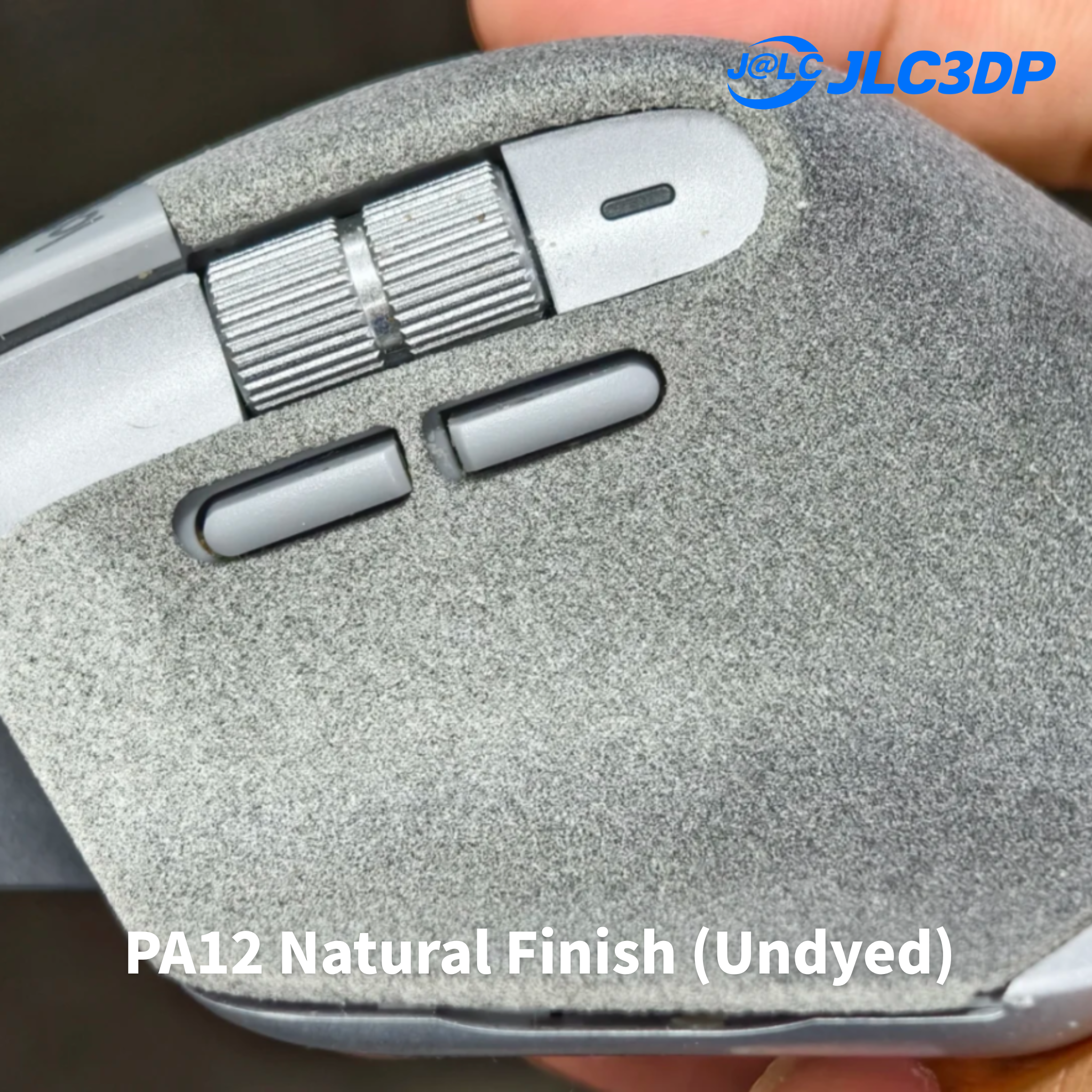
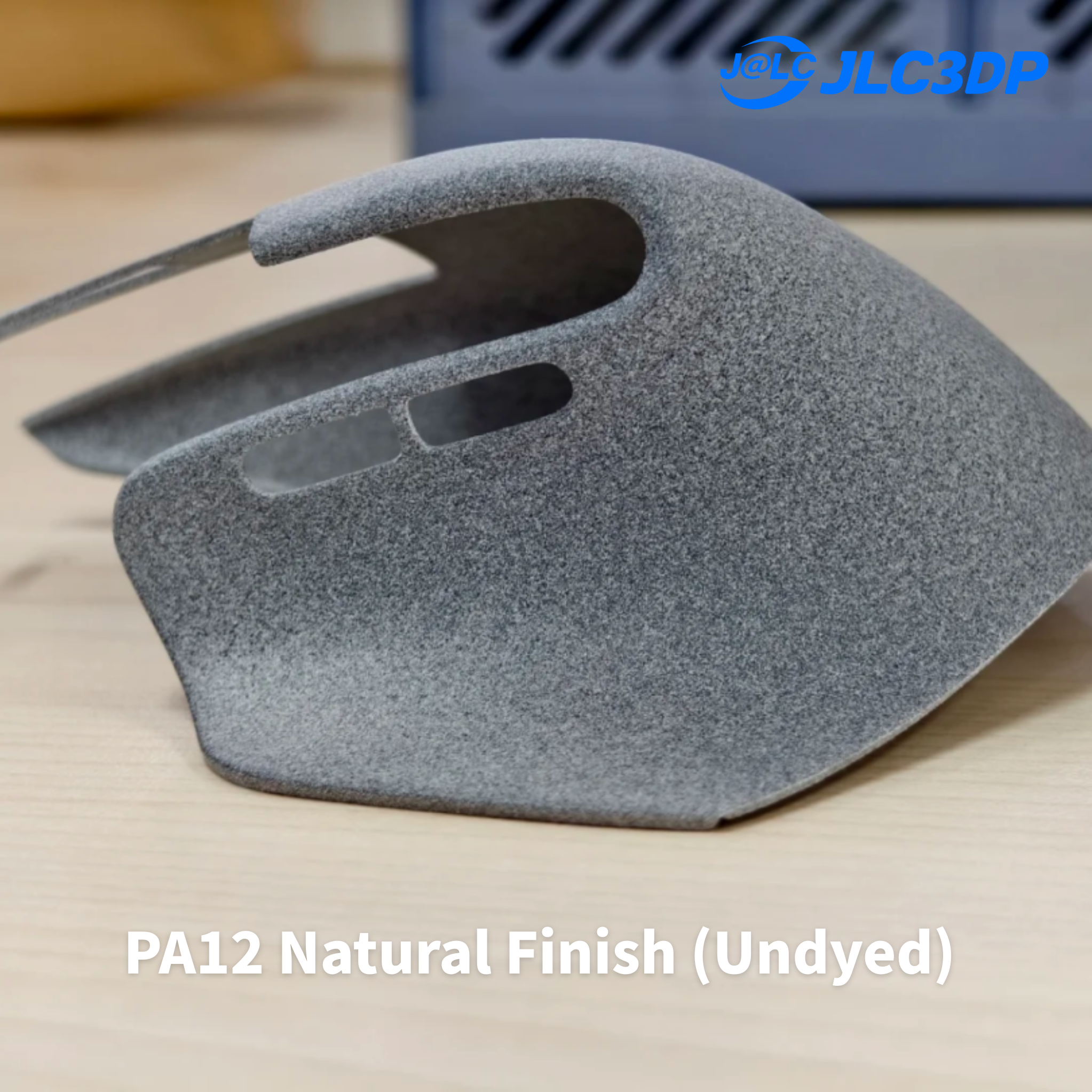
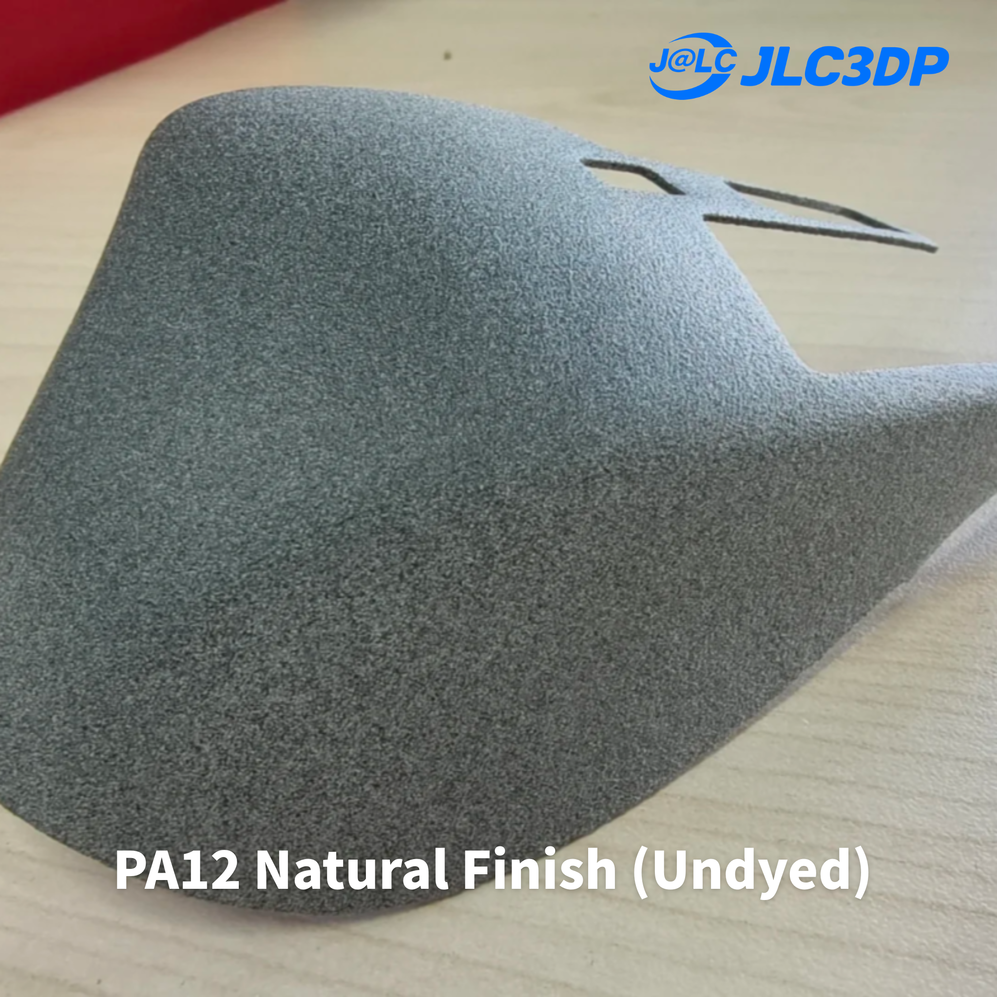
After 10+ years of heavy use, a well-worn mouse started peeling badly.
Replacing the original shell? Not cheap.
So the creator chose a PA12-HP Nylon 3D-printed replacement shell made with JLC3DP.
Why PA12-HP Nylon made sense:
• Smooth, slightly textured feel — comfortable for long sessions
• Durable enough for constant hand contact
• Clean natural finish, with optional black dye
• Far cheaper than replacing the entire device
Beginner-friendly repair workflow:
Model → PA12-HP Nylon print → B-7000 glue → shell swap
No special tools. No mods. Back in daily use.
💡 This is functional 3D printing in real life
Not a showcase part. Not a prototype.
Just extending the life of everyday gear.
This is a personal repair project, not an official replacement part.
🎁 PA12-HP Nylon currently has up to $28 in coupons, making small repairs even more accessible.
👉 https://jlc3dp.com/coupon-center?from=3dpsm
💬 Question for makers:
Would you repair your daily gear like this — or replace it?