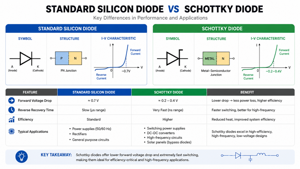
At first glance, a Schottky diode looks no different from an ordinary rectifier diode. Both allow current to flow in one direction while blocking it in the opposite direction. Because of this similarity, many beginners assume they can be used interchangeably.
Schottky diodes are designed for different priorities. They have a much lower forward voltage drop and switch significantly faster than conventional silicon diodes. These characteristics make them a popular choice in switching power supplies, battery-powered devices, and high-speed digital circuits where efficiency and fast response are important.
Choosing the right diode isn't simply about its current or voltage rating—it also depends on how quickly it needs to respond and how much power loss your application can tolerate.
Why Forward Voltage Matters
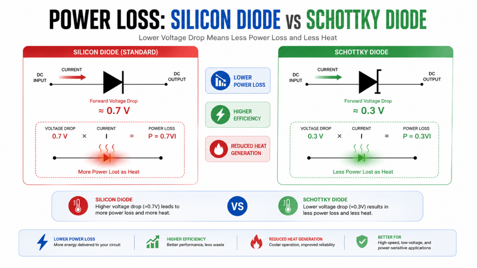
Whenever current flows through a diode, part of the electrical energy is lost as heat due to the diode's forward voltage drop.
For example, a standard silicon diode typically drops around 0.7V, while a Schottky diode usually drops between 0.2V and 0.4V, depending on the device and operating current. That difference may seem small, but in low-voltage circuits it can noticeably improve efficiency and reduce heat generation.
This is one reason Schottky diodes are commonly found in DC-DC converters, battery-powered equipment, and power distribution circuits.
Where You'll Commonly Find Schottky Diodes
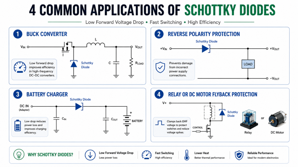
Because of their fast-switching speed and low forward voltage, Schottky diodes appear in many modern electronic products.
Common applications include switching regulators, reverse polarity protection, freewheeling diodes for inductive loads, battery charging circuits, and solar power systems. They're also widely used in portable devices where maximizing battery life is an important design goal.
While Schottky diodes offer many advantages, they usually have higher reverse leakage current than standard silicon diodes. This trade-off should always be considered when selecting a device for low-power or high-temperature applications.
Recommended Devices
The following Schottky diodes are widely used in embedded systems and power electronics:
| Device |
VRRM |
IF |
Typical Applications |
| 1N5819 |
40V |
1A |
General-purpose Schottky circuits |
| SS14 |
40V |
1A |
SMD embedded and IoT boards |
| SS34 |
40V |
3A |
DC-DC converters and power distribution |
| MBR1045 |
45V |
10A |
High-current power supplies and industrial applications |
Always verify the maximum reverse voltage, forward current, package type, and thermal requirements before selecting a replacement device.
Schottky diodes may look like ordinary silicon diodes, but their electrical characteristics make them better suited for many modern electronic designs. Understanding their lower forward voltage, faster switching speed, and practical limitations helps engineers choose the right diode for better efficiency and more reliable circuits.
#ElectronicTips# #ElectronicComponents# #SchottkyDiode# #PowerElectronics# #EmbeddedSystems# #CircuitDesign#



 Electronic Community