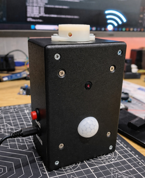
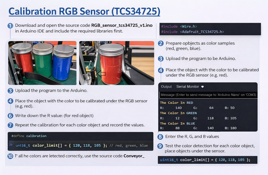
Electrostatic Discharge (ESD) protection is critical in electronic manufacturing environments where sensitive components are handled. A faulty wrist strap or improper grounding can silently damage microcontrollers, sensors, and communication modules.
To improve traceability and operational safety, an IoT-based ESD wrist strap tester was developed using ESP8266 with RFID authentication and web-based logging.
This system ensures that only registered personnel can perform ESD checks while automatically recording test results to a centralized database.
![]()
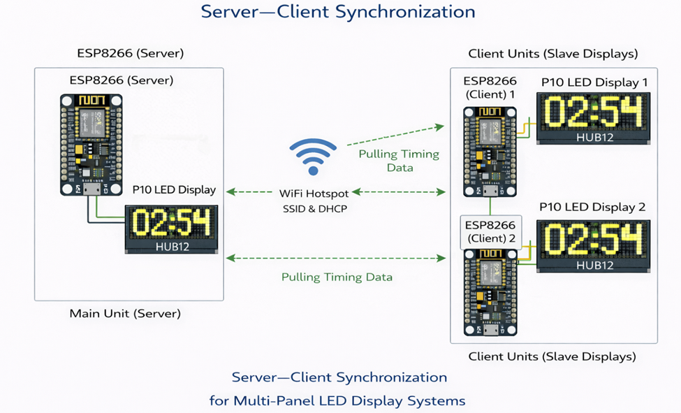
System Architecture Overview
![]()
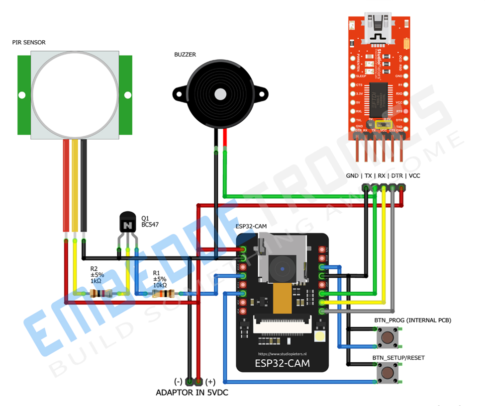
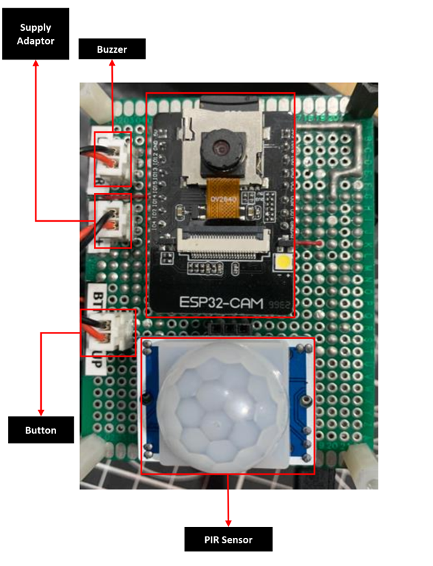
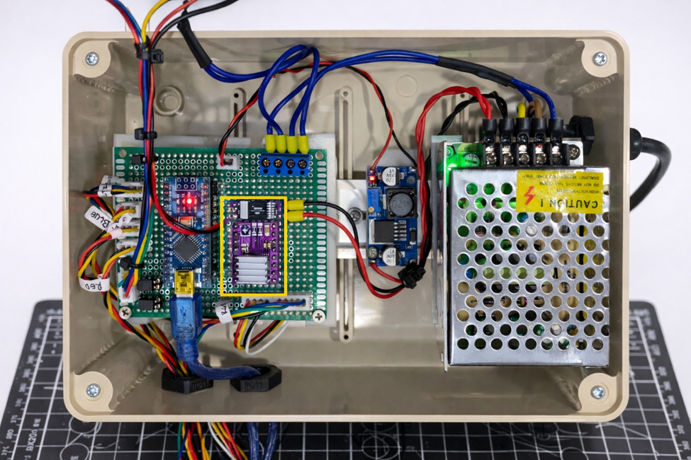
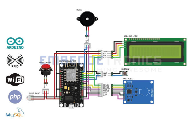
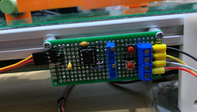
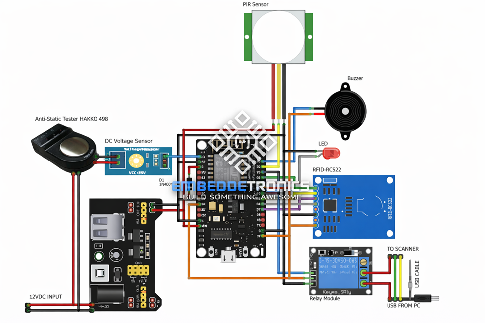
The complete hardware architecture is shown in the wiring diagram. The system consists of:
- ESP8266 (NodeMCU) as main controller
- Anti-Static Tester (HAKKO 498 type interface)
- DC Voltage Sensor module
- RFID RC522 module
- Relay module
- Buzzer and LED indicators
- PIR sensor (presence detection)
- 12V DC power input with voltage regulation
The ESP8266 acts as the central processing unit, coordinating authentication, test execution, data acquisition, and web communication.
RFID-Based Authentication
Before an ESD test can be performed, the user must scan an RFID card. The RC522 module reads the card UID and sends it to the ESP8266.
If the UID matches a registered user in the database:
- User identity is displayed on the web interface
- ESD test is enabled
- Test result is logged
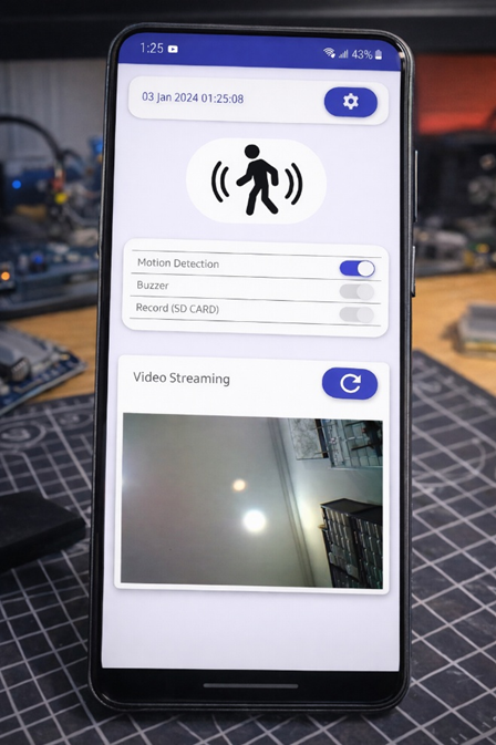
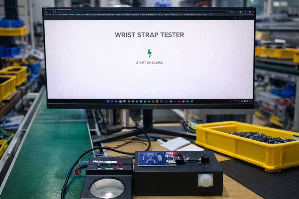
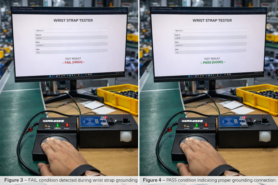
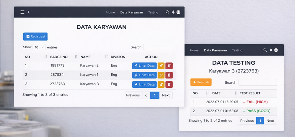
The operation interface shows the wrist strap tester display and user data fields, including:
- Badge number
- Name
- Division
- Test result
This ensures traceability and accountability in industrial environments.
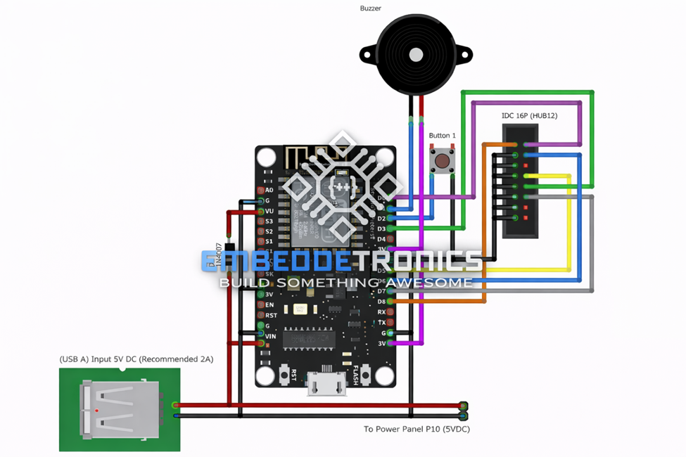
ESD Measurement Integration
![]()
The Anti-Static Tester output is connected to a DC Voltage Sensor module, which conditions the signal before it is read by the ESP8266 analog input.
The measurement flow is:
- User connects wrist strap
- Relay activates test path
- Anti-static tester measures grounding condition
- Voltage sensor captures test output
- ESP8266 evaluates result
- LED and buzzer indicate PASS or FAIL
This indirect sensing approach ensures electrical isolation and system protection.
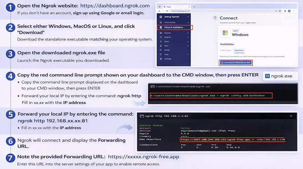
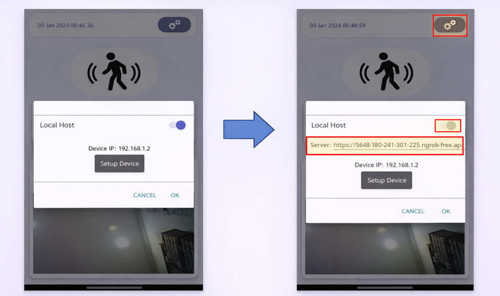
Web-Based IoT Logging
![]()
The ESP8266 connects to a 2.4 GHz WiFi access point and sends data to a local server hosted using XAMPP.
- Database is created in MySQL
- SQL file is imported
- PHP web interface handles login and employee management
- Admin can register new RFID cards
Each ESD test result is recorded in the database, enabling monitoring and reporting.
Relay and Interlock Preparation
The relay module shown in the wiring diagram is used to control the test activation path.
The system is designed so that:
- No authentication → Relay remains disabled
- Fault condition → Test blocked
- Power reset → System returns to safe state
This structure prepares the system for more advanced interlock handling logic, which will be discussed in the next article.
Electrical Protection and Stability
Because ESD testing environments involve high transient energy, several protective measures are implemented:
- Dedicated 12V input with regulation
- Diode protection on sensing line
- Proper grounding between modules
- Isolation via relay
- Stable 3.3V supply for RC522
These design decisions improve noise immunity and prevent false triggering.
Engineering Considerations
Key principles implemented in this system include:
· Authentication before activation
· Digital logging of all test results
· Hardware protection against voltage spikes
· Modular separation between sensing, control, and networking layers
This approach transforms a simple wrist strap tester into a smart industrial compliance system.
Conclusion
The IoT-based ESD wrist strap tester demonstrates how embedded systems can enhance industrial safety procedures. By combining RFID authentication, voltage sensing, relay control, and web-based logging, the system ensures controlled testing, traceable results, and improved operational discipline.
This project highlights the integration of embedded firmware, hardware protection, and IoT infrastructure within a real industrial application.
#ESDTester##ElectrostaticDischarge##IndustrialSafety##ESP8266##RFID##IoTProject##EmbeddedSystem##IndustrialAutomation##RelayControl##MySQLDatabase#