Why Not Use the Internal Clock?
Modern microcontrollers come with a built-in High-Speed Internal (HSI) RC oscillator. It is tempting to just use this and save board space. However, the HSI is notoriously inaccurate. It typically has a tolerance of around 1% to 2%, and worse, it drifts significantly as the temperature of the chip changes.
If your drone is flying in hot weather, that 1% error can cause high-speed communication protocols like CAN Bus, USB, and fast UART telemetry to completely desync, leading to dropped packets or a crashed drone.
For a fundamental breakdown of how quartz crystals generate stable frequencies compared to internal RC circuits, you can check on this website: Electronics Tutorials: Quartz Crystal Oscillators.
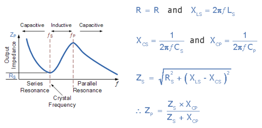
This images shown the exact, incredibly narrow resonance band that makes a quartz crystal so much more stable than an internal RC circuit
The 8MHz Crystal
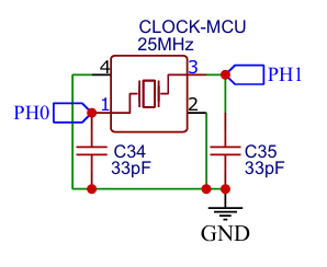
To achieve the parts-per-million (ppm) accuracy required for high-speed protocols, we must use an external quartz crystal. In my Flight Controller schematic, I use a dedicated 25MHz crystal connected directly to the OSC_IN and OSC_OUT pins of the MCU.
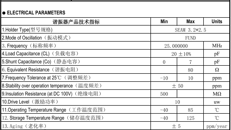
According to the specific datasheet for the crystal I selected, it has a strict Load Capacitance (CL) requirement of 20pF to operate at exactly 25.000000 MHz.
Why 30pF?
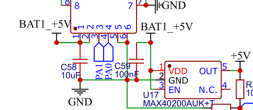
If you look closely at my schematic, you will see two small capacitors connecting each side of the crystal to Ground. These are "Load Capacitors." If these are the wrong value, your USB connection will likely fail to recognize the device.
How do we choose them? We calculate it!
The standard formula for calculating the external capacitors (C_ext) is:
C_ext = 2 * (CL - Cs)
"Cs" is the stray capacitance of your PCB traces and the MCU pins. For a standard, well-routed Flight Controller PCB, Cs is generally estimated to be 5pF.
Let's plug in our numbers:
C_ext = 2 * (20pF - 5pF)
C_ext = 2 * 15pF
C_ext = 30pF
Therefore, the mathematically perfect value for our load capacitors is 30pF.
However, in my initial schematic draft, I utilized 33pF capacitors. Is this wrong? Not necessarily! If we reverse the math, using 33pF capacitors means the circuit assumes a stray capacitance of exactly 3.5pF instead of 5pF. If your PCB traces between the MCU and the crystal are extremely short and well-optimized, 33pF will work flawlessly. But for the safest, sticking to the standard calculated 30pF is best practice!
STMicroelectronics AN2867
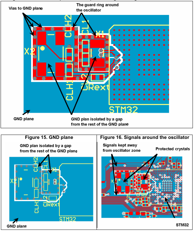
If you are designing a Flight Controller using an STM32 MCU, you cannot just guess these values or layout techniques. You must design the schematic according to the manufacturer's strict specifications.
The absolute best resource for this is the official STMicroelectronics Application Note AN2867: Oscillator design guide for STM8AF/AL/S, STM32 MCUs and MPUs. It dictates exactly how to select the crystal, verify the ESR, and route the PCB traces.
You can download and read the official document directly from STMicroelectronics here: STMicroelectronics AN2867.
Software Integration
Once the hardware is designed correctly, we tell our firmware to ignore the internal clock. In ArduPilot or Betaflight hardware definition files, we explicitly define the HSE frequency as 25.000.000 Hz. The software then configures the internal Phase-Locked Loop (PLL) multipliers to boost that 8MHz signal up to the MCU's maximum processing speed!