Managing Component Heat: When to Use Thermal Vias vs. Heat Sinks

Heat has the potential to destroy PCBs without producing any noise. If you ignore it, your circuit board will become unreliable and ruin your design. The big question really is how to deal with heat.

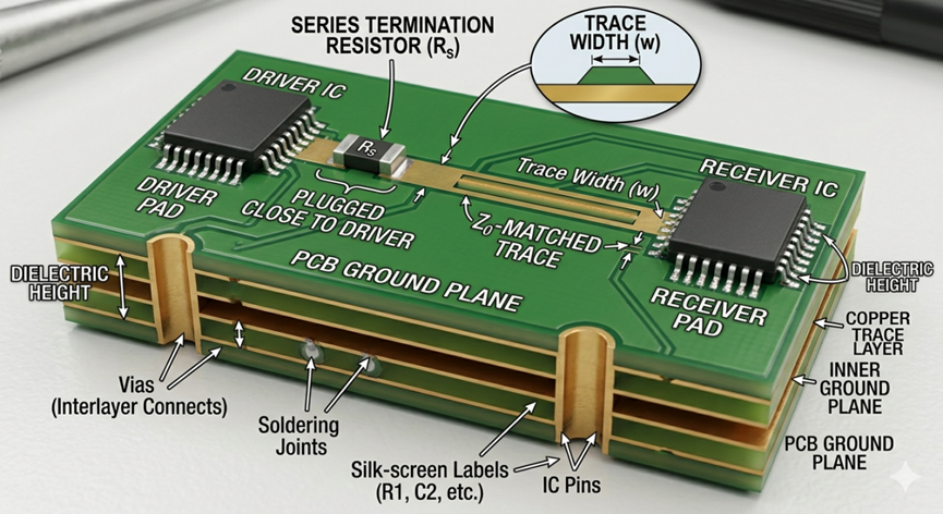
Thermal vias are your first line of defense. A thermal via is a small hole plated through to another layer of copper, typically used under or near heat-generating devices such as: regulators, power ICs, etc. Thermal vias transfer heat from the top layer of the PCB to the inner or bottom copper planes. They are small, inexpensive, and effective for transferring and dissipating moderate amounts of heat. A well-designed array of thermal vias—which have proper diameter, spacing and are connected to a large copper pour—will greatly enhance the capability of the PCB to dissipate heat without adding any additional board space.

image.png

PCB with thermal vias

However, thermal vias do have limitations. They are designed to transfer the heat to the PCB copper for distribution. If the PCB does not have adequate copper at the copper plane level(s) to dissipate the thermal energy in a time frame, the thermal energy will continue to place excessive heat on the thermal vias and eventually overheat the device.

This is where heat sinks come into play. A heat sink is a device that is designed to attach physically to the device being cooled and to increase the amount of surface area that will be able to dissipate thermal energy to the surrounding air. Heat sinks are extremely important for devices that generate a lot of thermal energy compared to the capacity of the PCB to dissipate the thermal energy. An example of this would be voltage regulators, power transistors, or LED devices.

image.png

PCB with thermal vias

The decision of whether to use thermal vias or a heat sink depends on the application requirements and the available space. In general, thermal vias and solid ground planes are adequate for compact designs such as wearables and IoT nodes. In high power applications, you can use both thermal vias to transfer heat away from the component and a heat sink to transfer heat to the air.

Airflow should also be taken into consideration when selecting a heat sink; heat sinks in an enclosed space without any form of airflow will not work well.

In conclusion: Thermal vias provide good heatsinking but are not as effective as using a full sized heat sink in a normal way. When used together, they ensure that you don't overheat your printed circuit boards.

image.png

PCB integrating heat sinks and thermal vias

PCB Design
How to Add Artistic Touches to Your PCB Using Silk and Copper

Why Are PCBs so boring with their whole size being a simple rectangle that is usually a dull color? That is changing quickly! With the right imagination, your board can function as both a functional art piece and an incredibly well designed product. Nothing says, “engineer with style,” more than having a well routed ground plane on your board.

The first thing you need to think about is your silkscreen layer, which will be your canvas for logos, labels and subtle design elements. Keep your designs to a minimum (not too high a density) because a high density design will probably get clipped when it goes to manufacturing. When you do design in your silkscreen, make sure you use the right line width, which is usually greater than or equal to 0.15 mm, and don’t put a silkscreen over the pads unless you enjoy having mysterious problems when you go to solder parts onto them.

image.png

PCB silkscreen layer, Logo printing

Next, begin the process of creating your copper artwork. By designing your copper pours or traces, you can design patterns, logos, and elaborate designs directly into the board. Exposed copper (using ENIG or HASL) can look great when combined with different colors of solder mask. However, don’t forget that copper will conduct electricity, and you will not like it if you create an antenna or short to ground with your logo.

image.png

Copper pour designs on PCB

To add some additional pizzazz, try using solder mask openings to expose areas of copper that are under the solder mask. Many companies will now also have various colors of solder masks to choose from such as black, red, or blue as well as some that have a matte finish. This can give you a lot more flexibility for the aesthetics of the board.

Layer alignment is important. If the layer artwork is not aligned properly, it may appear messy. Therefore, it is critical to preview your Gerber files thoroughly. Follow the manufacturer's minimum requirements of spacing and clearance between design components, because the graphics should not negatively impact how the piece functions.

Ensure that the graphic components serve a valid purpose. The artistic portion of the layout helps improve the useability of the overall layout (via clear labels, orientation indicators, and branding), whereas the graphic components merely serve as decoratively increasing the aesthetics of the layout. By designing your PCBs properly, you can have both an attractive and functional product.

image.png

well designed PCB with proper layer alignment.

After you have completed the design process correctly (note there is a long timeline for debugging we will be doing), you will now possess a printed circuit board that functions and appears suitable for display!

PCB Design
How to: choose between analog and digital LEDs for your project

When choosing LEDs for an electronics project, the decision between Analog and Digital (Addressable) is a crucial architectural choice that will influence your MCU’s workload and your power delivery strategy.

Analog LED

Analog strips are simple components. Every LED on the strip is connected to the same power lines, meaning they all change color and brightness simultaneously. To control these, your MCU uses Pulse Width Modulation (PWM). Since an MCU pin cannot handle the high current required by a strip, you must use external N-Channel MOSFETs as switches. The MCU toggles the MOSFET gates at high frequencies to dim or blend colors. On the bright side, they are inexpensive, extremely bright, and offer high color resolution limited only by your MCU's PWM timers. However, you lack individual pixel control, it's all or nothing. Wiring is also more complex for RGB because you need thick, dedicated wires for each color channel to handle the Amps.

Digital LED

On the other hand, digital LEDs, contain a tiny driver IC inside the LED package itself. These use a high-speed NRZ (Non-Return-to-Zero) serial protocol. The MCU sends a single data stream where each LED "consumes" its 24-bit color data and passes the rest to the next pixel. You can control every single pixel independently using just one MCU pin. This allows for complex animations and "chasing" effects which could be very impressive and fun for your projects. However, they are timing-critical. If your MCU's code is interrupted by a background task, the data signal can glitch. They also have a "quiescent current," meaning they consume power even when they are "off."

What should you choose?

Choose Analog for architectural lighting where uniformity is key and budget is tight. Choose digital for dynamic displays, but ensure you include a large filter capacitor (1000µF) across the power rails to prevent voltage spikes from damaging the sensitive internal ICs.

LED Project
How to: pick the right frequency for your oscillator

Try to think of the crystal oscillator as the "heartbeat" of your MCU, without a steady, reliable pulse (namely, the clock), the processor's "brain" simply can’t function. Most of the time, your design process is straightforward because the MCU manufacturer has already done the heavy lifting. If you check the datasheet, you’ll typically find a recommended part number or a list of specific requirements for frequency, Equivalent Series Resistance (ESR), and load capacitance (CL). When you're shopping for a crystal, you’ll see everything from 32.768 kHz to 50 MHz. So, how do you choose? It’s not always "faster is better."

Communication needs

First, look at your communication needs. This is the biggest trap. If you are using UART or CAN bus, you need a frequency that can be divided perfectly to hit standard baud rates (like 115,200 bps). If your clock speed is slightly off, your data will come out as gibberish. This is why frequencies like 7.3728 MHz or 14.7456 MHz exist, they actually divide perfectly into standard communication speeds with 0% error.

Power consumption

Next, you should consider power consumption. In the world of MCUs, Current = Frequency. If you run your chip at 48 MHz instead of 8 MHz, you’re going to drain your battery much faster. If your project just reads a temperature sensor once a minute, a high MHz crystal is just wasting energy.

MCU's limits

Finally, check your MCU's Limits. Every datasheet has a "Maximum Operating Frequency" section. Some chips can hit 100 MHz, but only if the voltage is high enough (e.g., 3.3V). If you’re running on a 1.8V battery, the silicon literally can't "flip" its internal gates fast enough, and you might be limited to a much lower MHz.

A little practical tip: you can start by identifying your fastest peripheral (USB usually needs 48 MHz, for example). If you don't have high-speed needs, pick the lowest frequency that keeps your code responsive.

#mcu# #layout# #pcb design# #frequency#

MCU
Why PCB layout matters for MCU: some tips

#mcu# #layout# #pcb design#

Ever had code that runs perfectly on a development kit but when you actually try it, it crashes on your custom PCB? It’s a nightmare, and the problem is almost always the layout. In the real world, traces aren't just "lines" on a screen as you already know, they have parasitic inductance and resistance that can ruin your signal integrity. When you're dealing with sensitive signals, the layout is arguably the most important part of your entire design.

  • To keep things stable, try to place your MCU centrally. This allows you to keep high-speed SPI or clock lines as short as possible, which is the best way to minimize EMI (Electromagnetic Interference).
  • And please, whatever you do, don’t skip the decoupling! Think of those 0.1µF capacitors as tiny energy reservoirs; you must place them right against the VDD pins to filter out high-frequency noise before it ever hits the silicon.
  • Also, don’t forget about your crystal oscillator. It’s the "heartbeat" of your system, and because it generates the clock for your MCU, it is incredibly sensitive. Keep it as tight as possible to the XTAL pins and surround it with a grounded guard ring. This acts as a shield, protecting those delicate oscillations from "noisy" components like switching regulators.
  • Finally, always use a solid ground plane. It provides the low-impedance return path your signals crave, preventing "ground bounce" and those mysterious random resets that drive engineers crazy.
MCU
Navigating the World of Educational robotics: an insider thought

I’ve participated in many educational robotics competitions over the years, and I’m convinced they are the single best way to introduce students to STEM. There’s something unique about solving engineering problems in a competitive environment, even if it's on a small scale, that transforms abstract concepts into real-world skills. If you are an educator in Europe looking to dive into robotics, the first challenge isn't building the robot, it's choosing the right arena. To help you decide, here is my honest take on the "Big Three" competitions based on my personal experience in the pits. Also it doesn't only foster the engineer area, but also all of the soft skills: they actually get to work in group, organize, divide in sub-teams and organize tasks, as well as travel.

1. RoboCup: The Professional Standard

Let’s start with the biggest and, in my opinion, the best: RoboCup. It is one of the most complete and inspiring ways to approach robotics education.

What makes RoboCup stand out is its range. It offers subcategories for every level, from RoboCup Rescue Line for beginners to RoboCup Industrial, where you’re essentially competing at a university level. I’ve personally taken part in the Rescue Line and Maze categories, and they are extraordinary. Seeing students spend hours tinkering and competing against peers from across the globe is pure magic.

  • The Vibe: Very serious and highly organized. It operates like a true championship at both European and World levels.
  • The Tech: Unlike other competitions, RoboCup encourages a "pro" approach. You aren't limited to kits; you can use Arduino, Raspberry and industry-standard chips.
  • The Trade-off: It is less "free-form" than others. The regulations are strict and specific, so while you need immense creativity to solve the problems, you must do so within a very rigid framework.

2. WRO (World Robot Olympiad): The Creative Alternative

The WRO is another massive worldwide competition, but it feels very different from RoboCup. If I’m being honest, WRO is often better suited for students who are just starting their journey in electronics and software.

The challenges change frequently and tend to be more "creative" in their themes and is actually very nice to explore also how technology and engineering can be creative. However, there is a distinct hardware ceiling:

  • The Hardware: WRO leans heavily into the LEGO ecosystem. This is great for accessibility, but for students who already have significant expertise, it can start to feel a bit "too easy."
  • The Goal: It’s a fantastic entry point. But if your students are ready to move toward professional-grade hardware used in the industry, they might eventually outgrow this format.

3. FIRST (Lego League / Tech Challenge)

If you are looking to build a pipeline that includes elementary and middle school students, FIRST is the way to go. While they have tiers for older students, their ecosystem is masterfully designed for younger ages. It’s less about "pure engineering" and more about the holistic experience of teamwork and themed challenges. It’s the perfect "on-ramp" to get kids excited about STEM before they move on to the more technical rigors of RoboCup. This is the only competition I have not taken part in so actually I can't get any insight thought about.

FINAL THOUGHTS

Choosing a competition depends on your students' current level and your school's resources. If you want to push them toward "real" industrial hardware and a professional mindset, RoboCup is my top pick. If you want to foster quick creativity and stay within a familiar ecosystem, WRO is a brilliant choice.

The most important thing? Just get them to the starting line.

Educational Robot Competitions
How to solder SMD components.

Ever feel like you need the steady hands of a neurosurgeon just to put a circuit board together? You’re not alone. As components get smaller and "legs" disappear in favor of tiny pads tucked underneath, the old-school soldering iron can feel a bit like trying to perform surgery with a hockey stick. Personally, that has been one of the main issues for me when approaching components always smaller.
But here’s the secret: SMD (Surface Mount Device) soldering isn't actually harder; it’s just different. Choosing the right technique depends entirely on what you’re building and how many tiny parts you're willing to chase across your desk with tweezers.

The Trusty Soldering Iron (Manual Hand Soldering)
Don't retire your iron just yet. For basic SMD components like resistors, capacitors, and LEDs (the 0805 or 0603 sizes), a standard iron is often the fastest way to go. The Technique is actually very simple.

You "tin" one pad first, slide the component into the molten solder with tweezers, let it freeze, and then hit the other side. For chips with many legs (QFP), you can use drag soldering, where you pool a glob of solder and drag it across the pins.

When to use it: Perfect for one-off prototypes, repairs, or when you only have a couple of components to swap. A little tip that I think is very useful: use flux. Then use more flux. It’s the "magic juice" that prevents bridges and makes solder flow like a dream.

Hot Air Rework

If you’re dealing with components that have pads underneath the body (like QFN or BGA chips), a traditional iron literally can't reach the solder. This is where hot air shines. How? You apply solder paste to the pads, place the component, and blast it with controlled hot air. The coolest part? Surface tension. If your placement is slightly off, the molten solder will actually pull the chip into perfect alignment.

When to use it: well, it's essential for complex integrated circuits (ICs) or when you need to "non-destructively" remove a component to fix a mistake.

Reflow Soldering (The "Batch" Method)
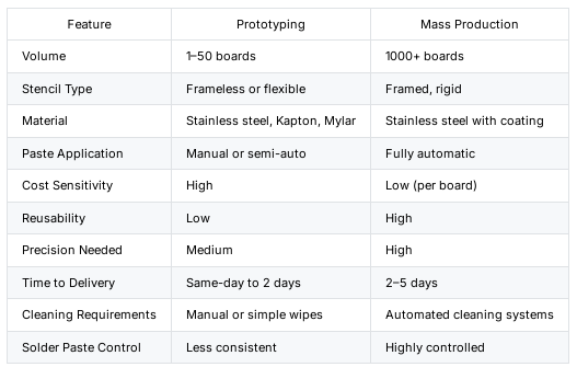
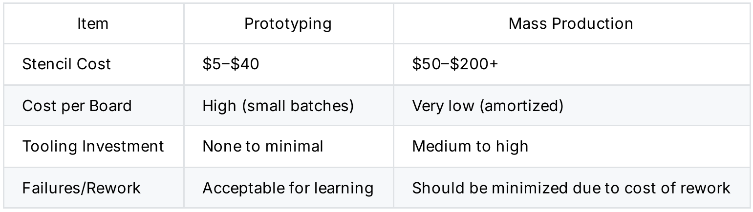
If you have a board with 50+ tiny components, soldering them one by one is a recipe for a headache. Reflow is how the pros (and advanced hobbyists) do it. Basically, you apply solder paste to the entire board using a stencil, "pepper" your components onto the paste, and then heat the whole board at once using a reflow oven or a dedicated hot plate. When to use it: Best for high-density boards or when you're "mass-producing" a small run of your project. It ensures every joint melts at the same time, leading to a much cleaner, professional look.

So actually the "best" technique is the one that keeps your frustration levels low and your joints shiny haha. If you're just starting out, grab some flux and a fine-tip iron. Once you start eyeing those tiny QFN chips, it’s time to level up to a hot air station.

8726892628246990848

#soldering#

Soldering Techniques
Designing Around Mechanical Constraints: Importing DXF to PCB.

Electrical engineers prefer clean schematics, while mechanical engineers have more of an appreciation for reality. Thus, DXF imports are utilized to help address the discrepancies between “this is how it should fit…” and “this does not fit…”

image.png

DXF file interface (generic)

A DXF file (drawing interchange file format) allows you to place mechanical outlines (such as panels, mounting holes and cutouts) directly into your PCB layout. Almost all professional EDA software products (KiCad, Altium, etc.) support the importing of DXF files onto a mechanical or keep-out layer of the PCB layout. By placing mechanical outlines onto a PCB layout before starting design with the electronic components, you are ensuring that the PCB will fit into the enclosure when it is manufactured, rather than negotiating aggressively with it after the fact.

image.png

DXF file interface (PCB design)

When first importing the DXF, you should do so on a mechanical or outline layer; do not import onto a copper layer unless you like chaos. The first thing to do once you have imported the DXF is to verify the scale of the file. Different DXFs can use different unit types. If the DXF file has not been set to the appropriate unit of measure, your PCB may physically fit but not necessarily work in our world.

Once you verify that the DXF file is properly scaled and in the correct file format, you can use the DXF to assist in designing your PCB outline, your mounting holes, and your keepout area. Additionally, be sure to align connectors, buttons and LEDs on the PCB with the openings of the enclosure. There’s nothing worse for an enclosure than to have a USB port hiding behind a piece of plastic, it will just give you a reason to design a revision “B”.

Take care when designing with tolerances; mechanical parts can vary from what designers expect just as PCBs can. Always provide clearance around all edges as well as holes so that tolerances can be accommodated for during manufacturing. A snug fit is preferable to force-fitting parts together and can significantly add to the cost of assembly.

At the end of your design process, you should lock the DXF layer so you do not risk accidentally nudging it while aligning other layers.

Communicate closely with your Mechanical Team as it is important to remember that DXF imports are not one-time activities. They are repeating processes that will need to be updated as your design goes through revisions and/or changes.

In summary, importing a DXF file allows for more precise placements when designing a PCB than would otherwise be done relying solely on “almost fits” when placing components on a PCB.

image.png

PCB design using DXF file

PCB Design
Understanding PCB Finishes: ENIG vs. HASL vs. OSP

Selecting a surface finish for a PCB can be like ordering a coffee: many options will work but what may appear to be similar at first can actually differ vastly when you consider all of the particulars.

image.png

HASL finished PCB

HASL (Hot Air Solder Leveling) is the most traditional surface finish option to use, as it first dips the board into hot liquid solder, then levels them with hot air afterward. It's a low-cost solution that produces an extremely durable surface finish; however, the surface will not be perfectly smooth after being leveled with hot air. That's perfectly acceptable for through-hole parts or for larger surface mount designs, but not ideal for using very fine-pitch parts. Think of HASL as being similar to a plain cup of black coffee: very simple, easy to depend upon, but somewhat rough around the edges.

image.png

ENIG finished PCB

ENIG (Electroless Nickel Immersion Gold) is considered the premium surface finish option. ENIG produces a very flat/smooth surface that provides excellent solderability, corrosion resistance, and is a great surface finish for BGAs and high-density surface mount designs. ENIGs drawbacks are that they cost significantly more than HASL and you will need to carefully control the ENIG processes to prevent defects, such as "black pad." Think of ENIGs being similar to a highly crafted latte: smooth, refined, and expensive.

image.png

OSP finished PCB

OSP (Organic Solderability Preservatives) is the simplest form of PCB board finishes and it provides copper with a protective coating which protects its surface from oxidation. OSP is inexpensive and provides a fairly flat surface but is not very robust and does not have a long shelf life. It may degrade after multiple reflows, so pay attention to how you handle it. OSP is like a cheap, fast coffee - works well, cheap and works most effectively when used quickly.

So, what should you use? If your project has a low budget and a simple design then HASL is acceptable. However, for a complex and dense design where the use of high-speed technology, ENIG will normally be the better option. In the case of producing large quantities of products (cost-effective and with strict quality control) OSP would be the best.

The type of finished surface of your PCB will affect not only the overall looks of your PCB but also the quality of solderability, reliability and manufacturability. So, select wisely and your PCB will be forever grateful (in silence).

PCB Design
Comparing ESP32 Variants: S2, S3, C3, and C6

A showdown of family members' opinions.

If the ESP32 lineup were a family group chat conversation, every variant would claim to be the "most optimized." Let's break down the family drama.

image.png

ESP32-S2

A minimalist approach, the ESP32-S2 provides a single core, Wi-Fi only, no Bluetooth. The ESP32-S2 is great for secure IoT applications, provides extensive hardware security features, uses low power, and provides stability without the excess noise of additional radios.

image.png

ESP32-S3

The ESP32-S3 is the high achiever. Its dual-core design has Wi-Fi + Bluetooth LE, provides support for vector instructions for use with AI/ML applications (i.e., tiny neural networks), and is ideal for edge AI, vision and USB applications. If your project has "smart" in it, this is likely the variant that is included.

image.png

ESP32-C3 and ESP32-C6

The ESP32-C3 is the efficient underachiever. It features a RISC-V core (instead of an Xtensa core), provides low power consumption and cost-effective Wi-Fi + BLE, and is a great choice for scalable deployments of IoT where cost matters, but performance cannot be far behind.

Each ESP32-C6 represents cutting-edge technology. Both can offer RISC-V-based SoCs and both devices also include 802.11ax (Wi-Fi 6) and Bluetooth LE 5 communications standards. This variant further allows for network efficiency in busy environments. Imagine smart homes where there are multiple devices connected, but they share bandwidth (as though they were quietly talking) instead of yelling.

Key points: All are good, but fit is most important!

  1.   S2: simple and secure but only has Wi-Fi capabilities
    
  2.   S3: best for advanced applications with power and AI functionality
    
  3.   C3: most affordable; good performance in RISC-V
    
  4.   C6 :advanced connectivity (Wi-Fi 6)
    

Prior to implementing sensors, it is critical to analyze the surrounding environment prior to implementing the described sensors. To create the various types of sensor nodes, choose an ESP32-C3. If you plan to use artificial intelligence within your devices, purchase an ESP32-S3. Those that need an ideal range of connectivity options in the future will want to opt for an ESP32-C6. Lastly, if you intend for your sensor nodes to provide exemplary reliability, then configure your devices to utilize an ESP32-S2.

#mcu# #esp#

MCU
Dual-Core Programming: How to Offload Tasks to Core 1.

Using dual-core microcontrollers, such as the ESP32 or RP2040, allows for parallel processing by running tasks on two independent processors. By taking advantage of Core 1, for non-time-critical, processor-intensive tasks, like sensor processing, display updates or filtering algorithms, you can improve the responsiveness of time-critical tasks, such as I/O operations, networking or user interface functions.

image.png

core seperation

The main idea behind utilizing dual core microcontrollers is to separate tasks. Core 0 is responsible for all interrupt, communication stack, and other latency sensitive tasks, where as Core 1 is responsible for all non-time critical, processor intense, or blocking tasks.

This separation of tasks reduces bottlenecks from occurring, and thus aide in eliminating watchdog processor reset occurrences. On platforms such as the ESP32 (FreeRTOS based platform), tasks can be pinned to specific cores. You can do this with the API call xTaskCreatePinnedToCore() to assign a task(s) to a specific core, which will improve execution predictability, and reduce contention created by other tasks.

image.png

inter-core communication

Inter-core communication is essential. Shared Global Variables should be avoided through the use of Queues, Semaphores or Mutexes to prevent Race Conditions Always protect your shared resources with synchronization primitives to maintain the integrity of the data.

Also, minimize the dependencies between tasks on the two cores as much as possible. The more independent a task is of another, the better it will run on its designated core. For example, if you were to have a single processor do all of the pre-processing of sensor data and then only send to Core 0 the final post-processed data; this would result in less overhead (communication) between two processed sets of data.

image.png

multi-core debugging

Debugging is quite difficult on multi-core systems. Multi-core systems contain many more types of problems which make debugging more difficult than single-core systems, i.e., Dead Locks and Priority Inversion etc… As a rule, you should verify that your application is functioning prior to debugging when transferring from single to multi-core.

You also will want to monitor CPU Utilization in relation to Core 1, Core 1 may be underutilized due to Priority not being distributed evenly. Proper scheduling of processes and testing of processes should ensure the efficient utilization of all cores.

#microcontrollers#

esp32 #esp32#

MCU