Stepper motors genralised idea

872444976716343705687244497671507189768724449768077795328

Stepper motors were one of those components I kept hearing about, especially in things like 3D printers and CNC machines—but I didn’t really understand why they were used everywhere until I actually started working with them.

The main reason is precision. Unlike regular DC motors that just keep spinning, stepper motors move in fixed steps. Most commonly, that’s 1.8° per step, which gives 200 steps for one full rotation. This makes them really useful when you need controlled movement without adding sensors.

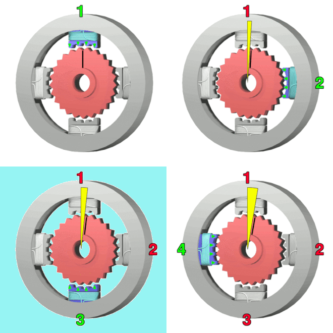
Internally, a stepper motor has a rotor (the shaft) and a stator with coils arranged in phases (usually A and B). By energizing these coils in a specific sequence, a rotating magnetic field is created, and the rotor keeps aligning with it. Instead of continuous rotation, it moves step by step.

One thing I initially misunderstood was microstepping. I thought it just increases the number of steps and gives more accuracy—but it’s a bit more nuanced than that.

With microstepping, instead of fully energizing one coil at a time, the driver controls current in both coils in ratios (like 50/50 or 75/25). This lets the rotor settle between full steps, making motion smoother and reducing vibrations. But it doesn’t necessarily mean you’re getting perfectly accurate “extra steps”—torque per microstep is lower, and there are nonlinearities.

Another thing that confused me early on was NEMA ratings. NEMA 17, NEMA 23, etc., don’t define performance—they only specify the physical size of the motor faceplate. Torque and current ratings can vary a lot even within the same NEMA size.

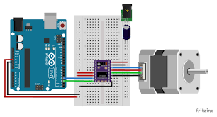
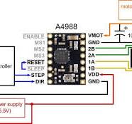
Drivers are also a big part of the system. Stepper motors aren’t just voltage-driven—you need drivers that regulate current properly. That’s where modules like A4988, DRV8825, and TMC2209 come in. Choosing the right one depends mainly on the current your motor needs and how smooth you want the motion.

Here are some common driver options and where they fit:

Driver Name Max Current Voltage Range Max Microstepping Best For
A4988 2.0A 8V – 35V 1/16 Budget NEMA 17
DRV8825 2.5A 8.2V – 45V 1/32 Higher voltage setups
TMC2209 2.8A (peak) 4.75V – 28V 1/256 Silent, smooth motion
TB6600 4.0A 9V – 42V 1/32 NEMA 23 / CNC
DM542 4.2A 20V – 50V 1/128 Industrial setups
DM860H 7.2A 18V – 80V 1/256 Large NEMA 34

stepper gif from https://www.wikipedia.org/

#electronics# #robotics# #steppermotor# #embedded# #engineering#

StepperMotors
Make your own Easy Buck converter: project for beginners

Hey there! if you’ve ever wanted to dive into the world of power electronics but felt intimidated by all the math and tiny components, this post is for you. In this post you will see how to build a high-efficiency buck converter, the magic device that takes a higher voltage (like from a battery) and steps it down to a lower voltage (like for your microcontrollers) without wasting a ton of energy as heat.

let’s break down how to design and build one of these as a beginner.

Why a buck converter? Well, linear regulators are easy, but they’re basically just fancy resistors that get hot. a buck converter uses an inductor and high-speed switching to be way more efficient. think of it like a dimmer switch for your power.

What you'll need (the bill of materials):

  • the controller: mc1068c buck regulator ic.
  • the inductor: 0.47μh (i used the mpl-al4020-r47 for its solid 12.5a saturation current).
  • resistors:
    • r1: 100kOhm
    • r2: 49.9kOhm (these set your output voltage via the feedback pin).
  • capacitors:
    • input: c1a, c2 (ceramic, 10μf to 22μf range).
    • output: c21, c22, c23 (we use multiple in parallel to keep the voltage smooth).
    • feed-forward: cff (a tiny 10pf cap to help with stability).
  • connectors: standard screw terminals or headers for vin and vout.

Layout tips

when you look at my PCB layout, you'll notice a few things:

  • keep it tight: the input capacitors (decoupling) and the inductor need to be as close to the ic as possible. this minimizes ringing and noise.

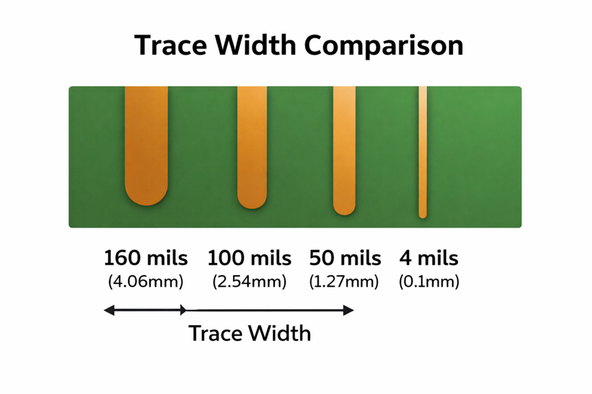
  • big copper: notice the thick traces? high current needs space to move, or your board will act like a heater.

  • ground plane: use a solid ground pour on the bottom layer. it acts as a shield and a heat sink.

    The layout is a begginer one! it has a lot of room for improving, what would you change?

Final thoughts

building your own power supply is a rite of passage. it feels pretty great when you plug in 5v, and a rock-solid 1.2v comes out the other side without a puff of smoke. Obviously the PCB layout is just a beginner project to get started with PCB design!

8724443605563088896

8724443605609226240

#POWERELECTRONICS# #PCB# #PCB# #JLCPCB#

Open Source Project
How to start with PCB Design if you only know basic electronics

Hi everyone! So I would like to share my personal experience designing PCBs as a beginner. So I have been designing PCBs for 3 years already and the most important thing I have learned in this period is that to start designing PCBs and actually get into that, you just have to choose a project and get hands-on.

  • First of all, look at some videos on-line, there are plenty, one example could be the following one: How To Start Video. Then, choose an easy project: it could be a simple LDO circuit, a buck converter, or a simple microcontroller activating some LEDs, and then start designing. For the software I would suggest EasyEDA just because for beginners it's the easiest one. Then just start designing the schematic! For the schematic I would say that the most important thing to keep in mind is: keep it organised and clean! For example, all the input pins on the left, outputs on the right, name the connections etc.. In this way it will be way easier to understand the schematic not only for you, but for whoever looks at it. I think that, by beginning to draw schematics with the good-practice guidelines in mind, you already have done a huge step ahead.
  • RUN THE DCR! (design rules checker) This is one of the most significant stept in my opinion, it allows you to not make huge mistakes!
  • After you have finished the schematic just go into the layout and routing! Just try and connect all the components as the software tells you by keeping in mind some easy rules: no 90 degrees angles, always keep it clean, don't be scared to use vias, use the right width for the traces, don't be scared to do something wrong it's perfectly normal. Personally, I think that designing PCBs just requires a lot of practice and attempts. Also EasyEDA has a lot of tutorials so if you need something just look there.
  • Once you have done some little projects, you can also try to do something more elaborate such a basic audio amplifier, or something that actually interests you. I think one of the best way to learn is do something useful for you and that you find exciting!
  • Finally, I would suggest you to print the PCB and actually test it. Even if you don't get to actually use it, having the product and actually testing it helps you understand what could you have done better. Also with JLCPCB printing the pcb is actually very cheap and the delivery is quite fast, so you don't need to have big capital to invest or something like that.

I will attach a little project (an LDO) I did as a beginner that might help you to get started. Since it was a PCB design I made as a beginner, it has some mistakes! What do you think they are? #PCBDesign#

8724422987732238336

8724422987727503360

PCB
Common Footprint Mistakes That Can Ruin Your SMT Order

The significance of a perfect schematic diminishes if your footprint is not accurate. In SMT assembly, even minor errors in the footprint can lead to costly production failures very rapidly.

image.png

SMT Assembly line/Pick and place

First of all, pad sizing errors are very common. Making solder joints can be weak when using pads that are smaller than what is needed. In contrast, when using larger pads you may experience loss of solder from tombstoning (when part of the electronics component lifts off of the printed circuit board). Make sure your land pattern matches the one recommended by the manufacture. This is the best method to achieve accurate solder joints.

image.png

Close-up of soldered SMD components

Secondly, make sure that there are no errors in pin pitch or spacing. Even a slight difference between pin pitches can cause the component not to fit. This is especially critical with fine pitch ICs such as QFN or BGA packages; tolerances for these components are very tight.

Another major issue is incorrect orientation of the footprint. If the pin 1 indicator is not aligned properly, an entire reel of components may be incorrectly installed, which may not be immediately obvious until the assembly is completed and tested.

Missing or unclear silkscreen markings are another piece of the puzzle that could cause assembly issues. You have a much lower probability of making a successful assembly if you can't find any obvious polarity markings (e.g. diodes, capacitors or chips).

Another reason for comparing parts in your design with their datasheet is that you can't assume that all parts that have a common part number will be compatible with each other with regards to the footprint. However, you should verify the footprint matching part number in the datasheet for all connectors and power parts.

image.png

PCB design software layout screenshot (conceptual)

Courtyard and clearance violations are two areas that are critical to any assembly process. If courtyards overlap one another, it may cause confusion with pick and place machines, or worse, actual assembly collisions.

The thermal design of a product is important; missing thermal pads on power ICs will cause them to overheat or have poor soldering, especially on packages designed to dissipate heat.

Also make sure to do a 3D assembly check before ordering the products, as doing so is beneficial to identify placement issues not found in the schematic or 2D layout.

PCB Design
How to Design a PCB for 20A Current Without Melting Traces

Designing a PCB for 20 A shouldn't be left to chance; it’s the result of sound engineering regarding heat, resistance, and copper management.

The first guiding principle is the importance of trace sizes. For example, according to IPC guidelines, a 20A trace on an external conductor (2 oz of copper per square foot) experiencing a temperature rise of 10 °C will require approximately 2.6-3 mm in width. Anything narrower than 2.6 mm will eventually heat the trace enough to melt, rendering it a fuse.

image.png

PCB copper traces close-up

The second principle is that you should always use the largest-gauge copper conductor you can. For example, if you are switching from 1oz copper conductors at 20A to 2 oz or larger-gauge copper conductors, you will substantially reduce the resistance and heat generated by the conductor. Think of this as increasing the water pipe's diameter and reinforcing the walls.

The third principle is to avoid the use of thin trace conductors completely; instead use copper pours or planes. Distributing the current over a larger surface area improves thermal performance by reducing hot spots and increasing the area available to dissipate excess heat, thereby also reducing voltage drop.

The fourth guideline is to use the shortest and most direct trace routing possible. Any time you lengthen a trace, you will substantially increase the resistance (R= ρL/A), which in turn will increase the heating and the voltage drop. Therefore, try to keep your high current paths as short as possible.

The fifth suggestion is to consider the use of multiple vias when routing power as a single via can cause a current bottleneck; Thus, to properly share the load and dissipate heat create multiple vias in parallel when the current load permits.

image.png

High-current PCB / power electronics

Finally, be aware of your thermal strategy. External traces will have better cooling characteristics than internal traces, and also the use of airflow and copper planes can greatly enhance the amount of current a trace can carry.

What’s the takeaway? When designing for 20A isn’t making sure there is a single “perfect trace width”; it’s increasing cross-sectional copper and minimizing resistance throughout the entire length of the trace. By doing this, your board should stay cool, perform well, and not melt.

image.png

Trace width comparison

PCB Design
Star Grounding: The Ultimate Way to Reduce Analog Noise.

If you’re experiencing noise, unpredictability, or overall annoyance when working with an analog circuit, it’s probably due to the method used to ground the circuit; not because of any components. Enter star grounding, which is a rather straightforward way of helping to significantly improve your signal by reducing interference.

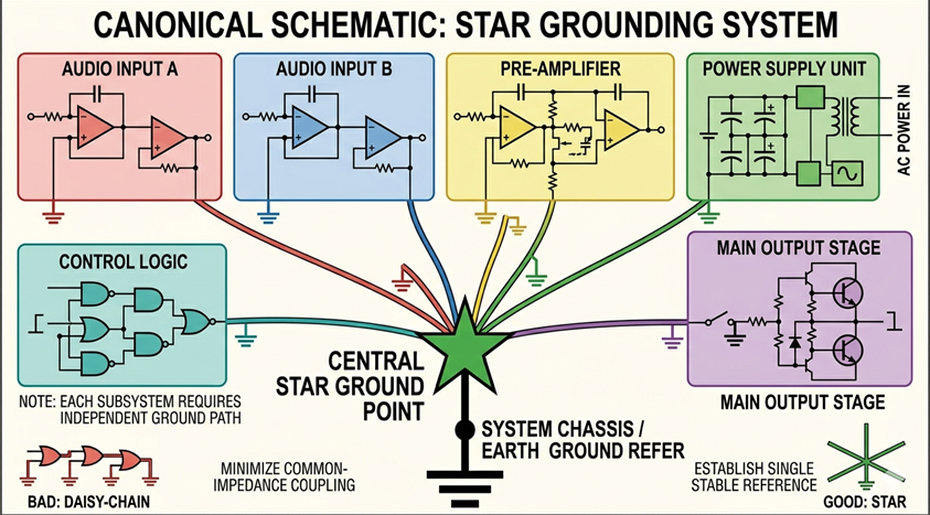
Star grounding connects all ground returns from the circuit(s) to a single central connection point instead of allowing current to flow through shared paths. The primary benefit of this method is that, because multiple circuits share ground paths (resulting in mixed return circuit currents), the mixing of return circuit currents generates voltage drops – or noise – when there is a shared circuit of low-level analog and/or high-level digital signal.

image.png

Canonocal Star grounding Schematic

Think of the shared path as a street that is shared by all return currents (mixed) at which to get to their destination (central star point). A street that has only one lane will be very congested; whereas, multiple streets with only one lane each will not be congested.

image.png

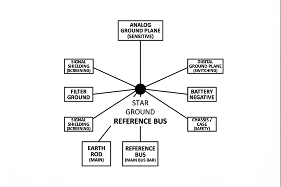
Star Grounding Reference Bus

In mixed-signal designs (digital switching noise and fragile analog signal), this becomes critical, as analog and digital signals can and will interfere with one another.

In practice, star grounding separates high-current (power stage, motor) and low-level analog (sensor, amplifier) returns by creating pathways from each section back to the central star point; thereby reducing the amount of interference. This becomes especially crucial with systems that use precision components, such as an operational amplifier circuit; as even a small voltage change (due to movement of the common ground point) will create distortion in the measurement.

But star grounding will not solve all problems. On newer multilayer printed circuit boards (PCBs), such as those designed with easyEDA Pro, using a solid ground plane typically has better electrical performance than a star ground layout due to having lower impedance return paths. Understanding which approach to use in what situation and when they can be combined is critical.

So if you’re dealing with analog noise, don’t first blame the components of your design. Instead, reevaluate how you have established ground on your PCB. A star ground properly implemented can sometimes mean the difference between a clean signal and hours of aggravating debugging!

image.png

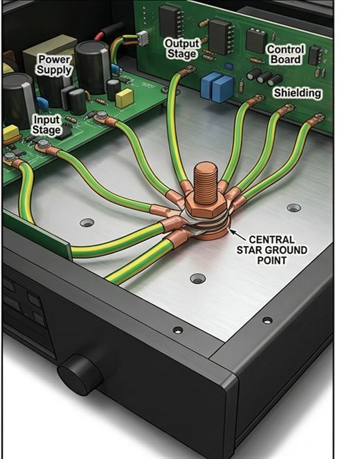
General star grounding

PCB Design