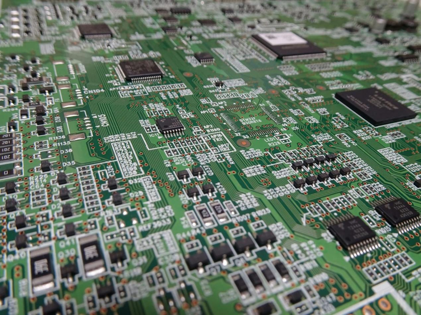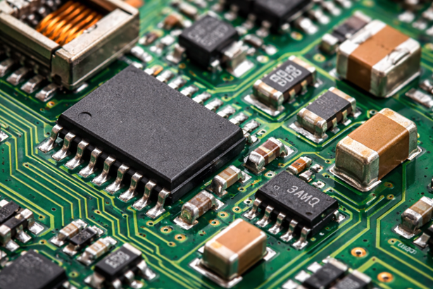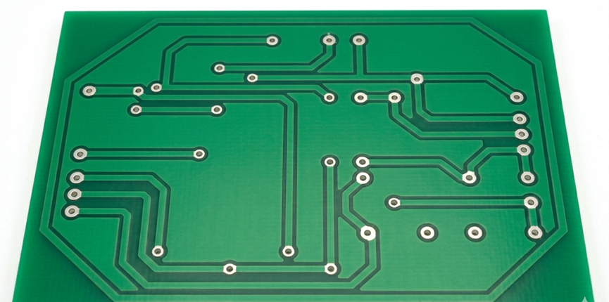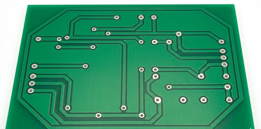
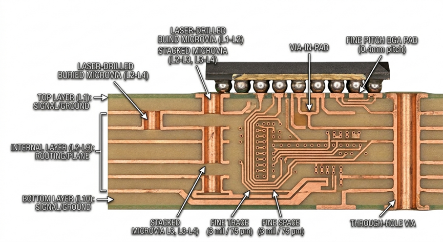
PCB trace close-up (conceptualized)
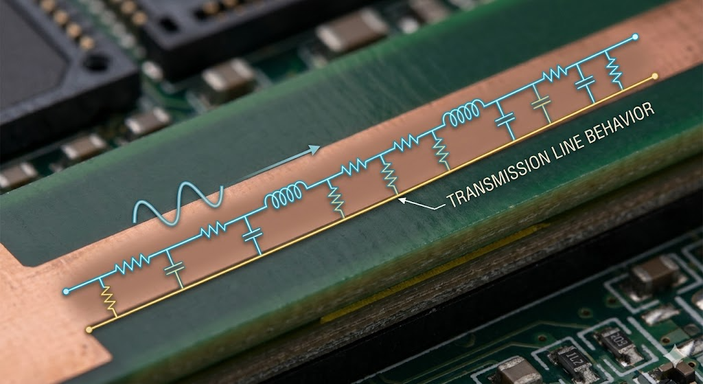
Signals, in PCB design, are not instantaneously transmitted, but rather propagate as electromagnetic waves over copper traces, which is fundamental to understanding why trace-length can be critical to signal integrity.
The speed at which a signal propagates depends on the material in which the signal is propagating, with typical standards for FR-4 PCB materials being approximately 50-70% of the speed of light. Thus, a signal propagating from one PCB pad to another may take 100 + picoseconds to travel a nominal distance of 2-3 centimeters. This travel time is relatively significant when compared with the fast rising (edge rate) of the signal itself.
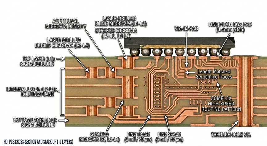
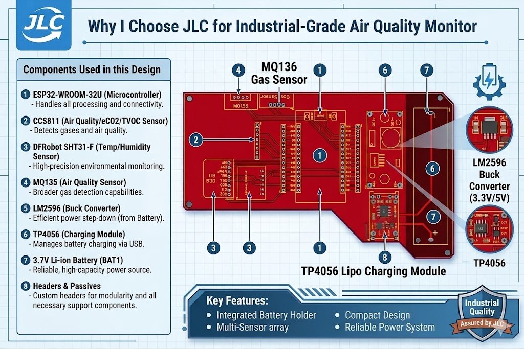
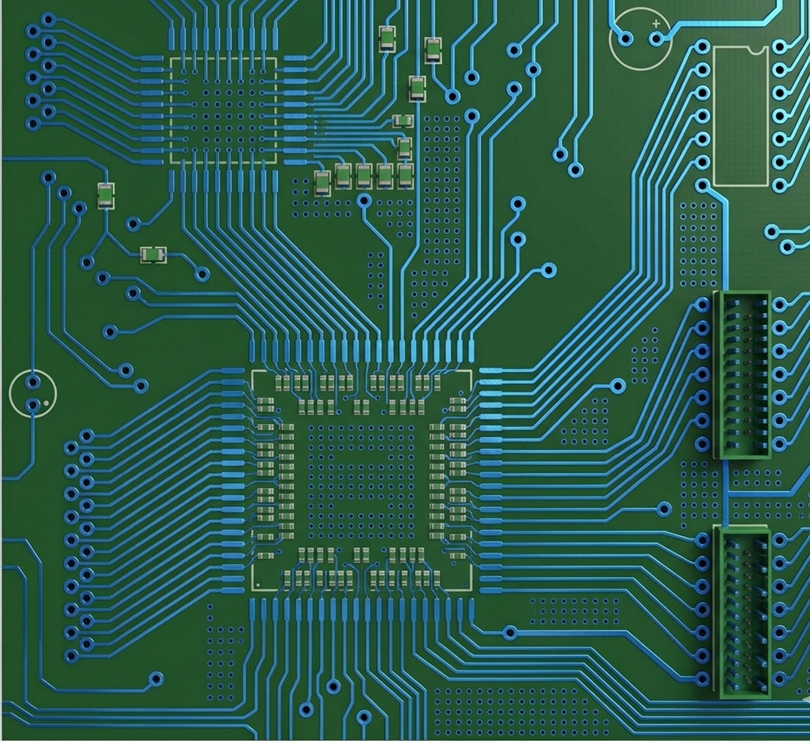
High-density PCB routing
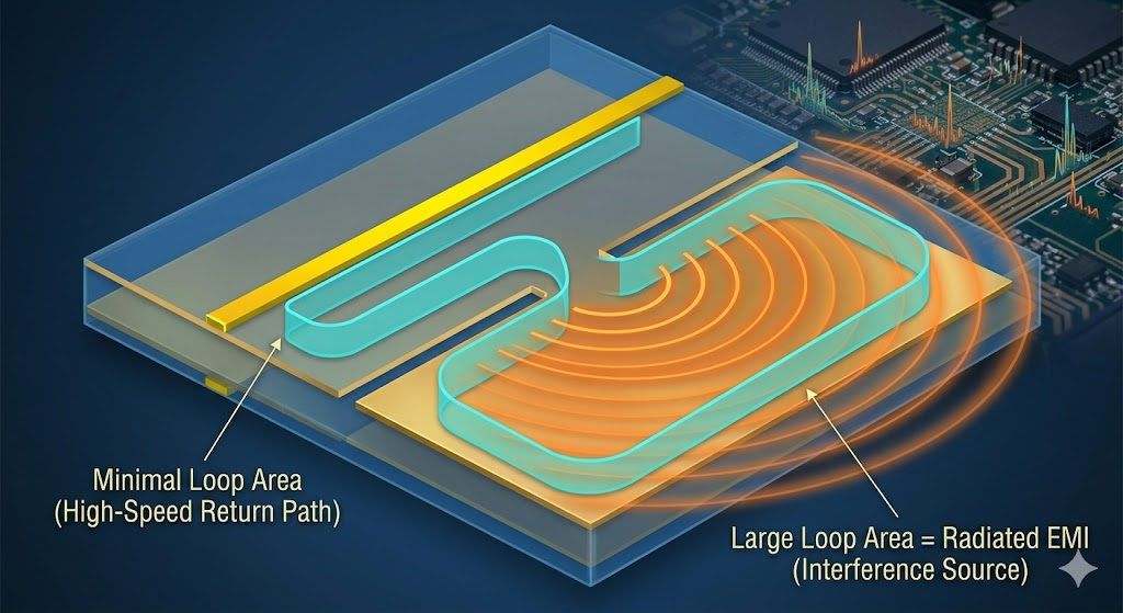
In addition to the delay of a signal traveling on its forward path, the signals also have a return path back to the source, typically by way of a common ground. Increased trace lengths create larger return loops, therefore increasing the inductance and the effects of voltage/potential noise from any external electromagnetic interference (EMI) sources.
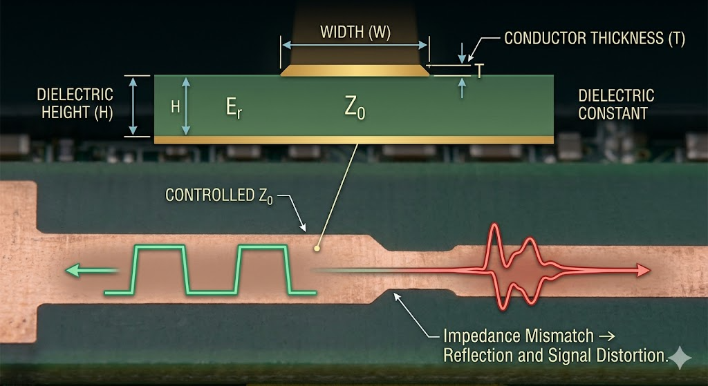
Higher trace lengths increase resistive/capacitive characteristics, which in turn may attenuate the signal, create longer rising/falling signals, and create potential distortion. When considered at higher frequencies, traces can behave like transmission lines, where impedance mismatching effects create reflections. Reflections can introduce ringing, as well as logic errors.
Timing is another major consideration. When considering buses or high-speed interfaces, a difference in trace length will cause some skew (i.e., signal arriving at different times). This will potentially cause the system to lose its intended relationship of synchronization for such devices as memory or differentials.
The reason designers apply techniques such as length matching, controlled impedance routing, and appropriate terminations is because keeping traces as short, direct, and grounded to the reference plane will help to maintain the integrity of the signal.
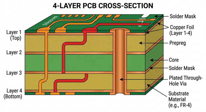
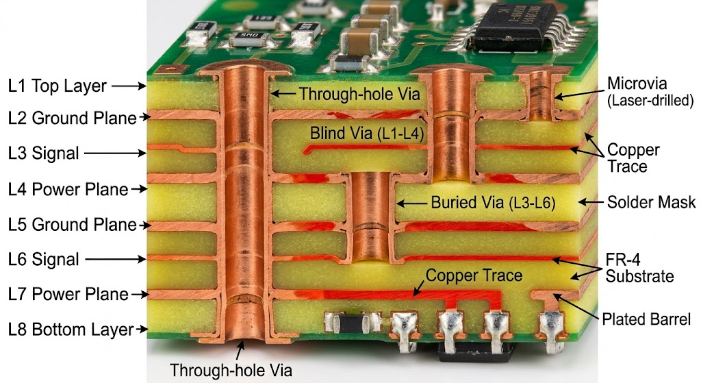
PCB with short, direct, and grounded traces
Takeaway? Trace length is not simply an attribute of geometry; it impacts the manner in which the signal behaves. As speeds continue to increase, propagation management is critical to reliable and predictable circuit operation.


 Electronic Community