The AMS1117, is it Good Enough for Your Flight Controller?

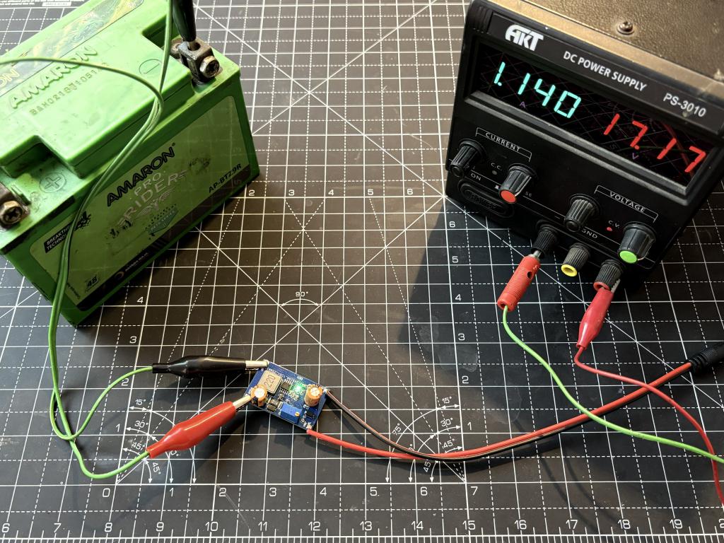
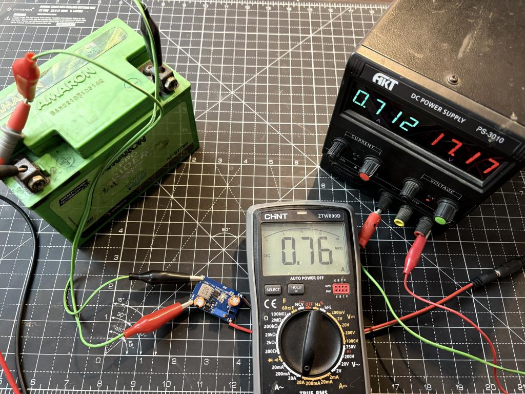
In my journey building flight controllers, I have seen many designers default to the AMS1117. While it is a "workhorse" for basic digital projects, using it to power a precision flight controller is like putting a noisy lawnmower engine into a luxury car.

1775570284679236388397022368995.jpg

If you want your EKF to be stable and your sensor to be accurate, you need a "Silent" power rail. Here is how I explain the shift from basic regulation to professional power integrity.

The AMS1117 Problem: Why it is "Dirty"

17755702253204081620965438544182.jpg

The AMS1117 is a linear regulator, but it is not a "Low-Noise" regulator. For a drone engineer, it has three major flaws:

  • High Dropout Voltage: It usually requires about 1.1V to 1.3V of "headroom." If your battery drops, your 5V rail might dip, causing your 3.3V sensor rail to brown out.
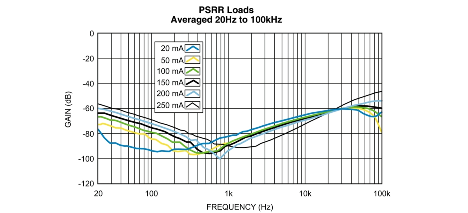
  • Poor PSRR: Power Supply Rejection Ratio (PSRR) measures how well the LDO blocks noise from the input (like ESC switching noise). The AMS1117 has a low PSRR at high frequencies where motors operate.
  • High Output Noise: It generates its own internal electrical "hiss" which can confuse the sensitive ADCs in your IMU.

Ultra-Low Noise LDOs

When I design a professional FC, I look for LDOs specifically marketed as Ultra-Low Noise or High PSRR. Examples the LP5907 or MIC5219.

You should look for:

  1. PSRR (dB): Look for values above 60dB or 70dB at 10kHz. This tells you the LDO is an active filter against motor noise.
  2. Noise (uVRMS): A silent LDO should have an output noise below 10uVRMS (from 10Hz to 100kHz).
  3. Accuracy: Look for 1% or 2% output voltage accuracy to ensure your sensors always see exactly 3.3V.

This images shown the PSRR vs. Frequency graph in an LDO datasheet. This curve illustrates how effectively the regulator blocks noise at different motor RPM frequencies.

8729859416052142080

Designing the "Silent" Rail Architecture

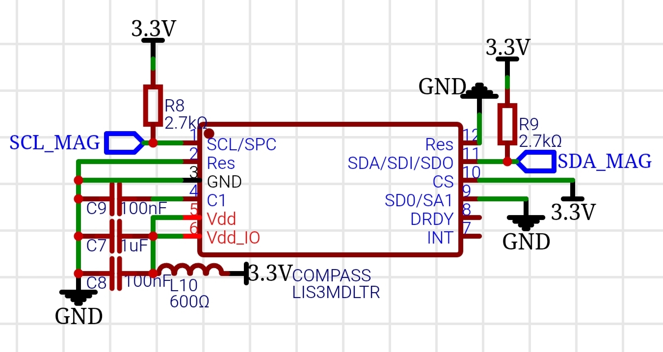
An LDO alone is not enough. You must build a Pi-Filter (C-L-C) to protect your sensors.

17755710369981065171610928000100.png

Here is the standard implementation I use for the 3.3V rail. The Component Recipe:

  • Input Bulk Capacitor:22uF tantalum or high-quality ceramic. This handles the "big" ripples from the main battery.
  • The Ferrite Bead: Use a 10uH or 600Ohm (at 100MHz) ferrite bead between the LDO and the sensor. This acts as a wall against high-frequency RF noise.
  • Output Decoupling: Use a combination of 10uF (for stability) and 100nF (for high-frequency spikes).

Layout

In my experience, the schematic is only 50% of the work. The other 50% is the PCB Layout.

  • Ground Planes: Use a solid Ground Plane. Do not "snake" your ground traces.
  • Kelvin Sensing: Place your output capacitors as close as humanly possible to the Vdd pins of your IMU and Compass.
  • Isolation: Keep the noisy AMS1117 (if used for LEDs or non-critical parts) on a completely different side of the board from your sensor LDO.

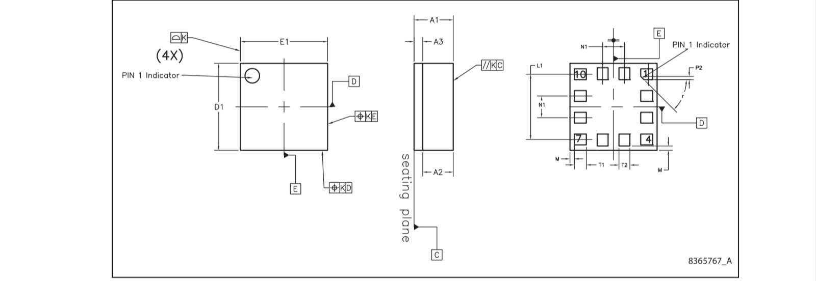
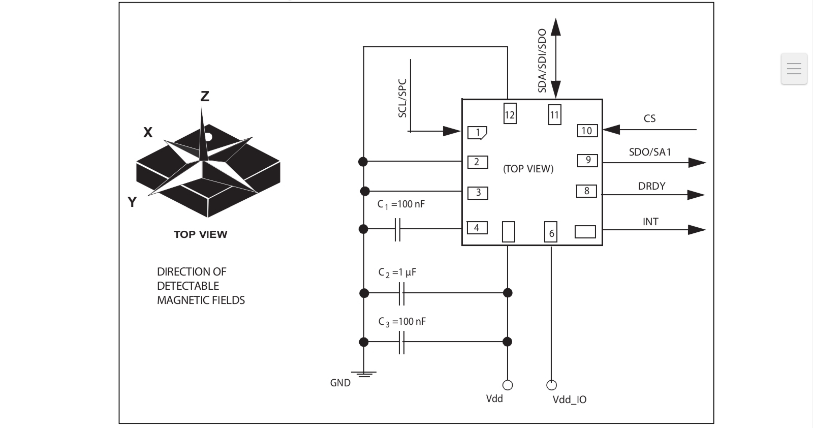
VFLGA-12 package outline and pin indicators to assist in correct PCB footprint design.

8729862722698539008

Recommended Resources

Professional Websites

Journals and Papers

  • "Power Supply Noise Reduction in Sensor Systems": Search this on** IEEE Xplore**. It explains why high-frequency noise causes "bias instability" in gyroscopes.
  • "System-on-Chip (SoC) Power Integrity": While advanced, this journal content explains the importance of decoupling capacitors like the 22uF and 100nF combo I mentioned.
DroneRacing
Kalman Filter in for State Estimation in UAV

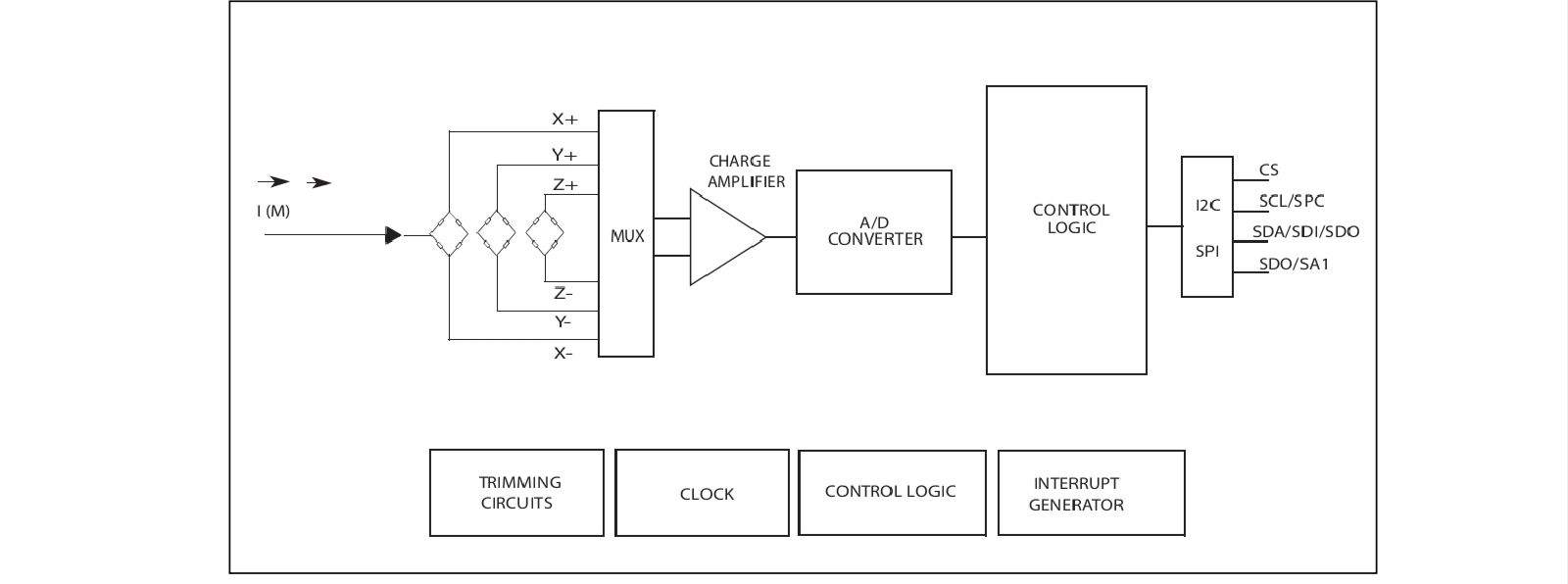
In my previous guide, I showed you how to design a high-redundancy Flight Controller (FC) using 2 IMUs and 2 Barometers. But having multiple sensors is useless if the "brain" doesn't know how to merge their data. If one IMU is vibrating and one Barometer has a pressure spike, which one should the drone trust?

This is where the Extended Kalman Filter (EKF) comes in. It is the gold standard for state estimation in modern UAVs.

What is EKF and Why "Extended"?

17755463080278028321740502195582.jpg

A standard Kalman Filter works perfectly for linear systems. However, drones are non-linear; rotating a drone by 90 degrees involves trigonometry (sin, cos), which creates curves, not straight lines. The Extended part of the EKF uses a mathematical trick called "Linearization" (usually via a Jacobian matrix) to handle these complex movements.In your custom FC, the EKF performs three main tasks:

  • Estimation: It guesses the drone's position, velocity, and orientation (Attitude).
  • Prediction: It uses your IMUs (Accelerometer and Gyroscope) to predict where the drone will be in the next millisecond.
  • Correction: It compares that prediction with "Truth" sensors like your Compass, GPS, and Barometers to fix any errors.

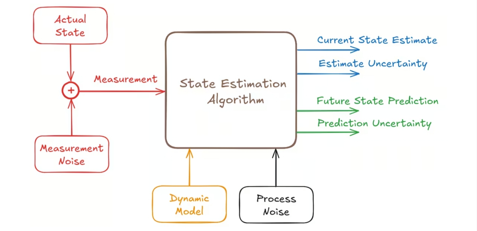
This images shown the basic loop of a Kalman Filter: Predict (Time Update) and Correct (Measurement Update).

8729757904172675072

Managing 2 IMUs and 2 Barometers

When you have a redundant setup like the one I designed, the EKF becomes a "Manager." Most advanced firmwares (like ArduPilot or PX4) actually run multiple EKF instances simultaneously.

IMU Blending

The EKF calculates the Innovation for each IMU. Innovation is simply the difference between what the IMU says and what the other sensors (GPS/Baro) expect.

  • If IMU1 has high vibration, its Innovation Variance will increase.
  • The EKF will automatically "weight" the data more toward IMU2.
  • This prevents a single sensor failure from causing a "flyaway."

Barometer Voting

With 2 Barometers, the EKF compares the pressure altitude. If one Barometer is placed near a hole in the frame and experiences "wind buffeting," the EKF detects the noise and relies on the cleaner Barometer.

Key Parameters for Your Code

When programming your EKF, you need to define Noise Density for your specific hardware. For example, if you are using an ICM-42688-P or MPU6000, you should look at the "Spectral Noise" section of the datasheet.

Parameter Recommended Value (Standard Units)
Gyro Noise 0.005 deg/s/sqrt(Hz)
Accel Noise 0.5 m/s/s
Baro Noise 2.0 meters
EKF Period 10ms

If you use a decoupling capacitor like a 22uF or 100nF near the IMU power pins, you can lower the "Noise" value in your EKF code, making the drone much "snappier" and more stable.

This images shown the Noise Density table in an IMU.

17755474087344122880379041491009.png

Implementation Resources

To truly master EKF for your project, I highly recommend studying these professional resources:

Technical Documentation

ArduPilot EKF3 Wiki: The best practical guide on how EKF handles multiple IMUs.

Website: https://ardupilot.org/dev/docs/ekf.html?hl=id-ID

PX4 Estimation Guide: Excellent explanation of the 24-state EKF.

Website: https://docs.px4.io/main/en/advanced_config/tuning_the_ecl_ekf

Journals and Academic Papers

"A New Approach to Linear Filtering and Prediction Problems" by R.E. Kalman (1960). This is the foundational paper.

DroneRacing
Compass in Flight Controller? Is it Necessary?

Building your own Flight Controller (FC) is a major milestone for any drone engineer. While gyroscopes and accelerometers (the IMU) provide stability, a magnetometer often called a digital compass to provides the "sense of direction" necessary for autonomous flight.
Here is a guide on why and how to integrate the LIS3MDL magnetometer into your custom flight controller project.

Why Do You Need a Compass in a Flight Controller?

A gyroscope can calculate orientation, but it suffers from drift over time. Without a reference point, the drone's heading (Yaw) will slowly rotate in the software even if the drone is pointing straight.

  • Heading Accuracy: The magnetometer uses the Earth's magnetic field to provide an absolute North reference.
  • Autonomous Navigation: For features like "Return to Launch" (RTL), Position Hold, or Waypoint missions, the FC must know exactly which way it is facing to move toward a coordinate.
  • GPS Limitation: A GPS can tell you where you are and your ground speed, but it cannot tell you which way the drone is "nose-in" while hovering.

This image illustrates that a drone can move forward while facing sideways; the compass tells the FC the "facing" direction.

8729745827399921664

The Challenge: Magnetic Interference

The biggest mistake in FC design is placing the magnetometer "on-board" near high-current components.

  • High-Current Wiring Effects: According to the LIS3MDL datasheet, high current in wiring and printed circuit traces can cause significant errors in magnetic field measurements.

  • The 10mA Rule: Conductor-generated magnetic fields add to the Earth’s field. You must keep currents higher than 10 mA at least a few millimeters away from the sensor.

  • EMI Sources: Motors, ESCs, and battery leads create massive electromagnetic interference (EMI).

Design Pro-Tip: Follow the "Cube Orange" or "Pixhawk" architecture. They often use a multi-PCB stack where the sensitive sensors (like the LIS3MDL) are separated from the power distribution and noisy IoT/Microcontroller logic.

LIS3MDL Magnetometer

17755440207408462014001821911745.jpg

The LIS3MDL is an ultra-low-power, high-performance 3-axis magnetometer. It is ideal for custom FCs due to its flexibility.
Key Specifications:

  • Selectable Full Scales: ±4/±8/±12/±16 gauss.

  • Digital Interfaces: Supports both I2C (standard and fast mode) and SPI interfaces.

  • Operating Voltage: 1.9 V to 3.6 V.

  • Resolution: 16-bit data output.

8729748207818571776

Hardware Installation & Schematic Guide

To integrate the LIS3MDL into your flight controller, follow the standard I2C implementation as shown in my provided schematic.
Wiring the LIS3MDL (I2C Mode)

8729750399145144320

To enable I2C mode, the CS (Chip Select) line must be tied high to Vdd_IO.

Pin # Name Function Connection
1 SCL/SPC I2C Clock To MCU SCL
11 SDA/SDI/SDO I2C Data To MCU SDA
10 CS Mode Select Tie to 3.3V (Logic High)
9 SDO/SA1 Address Select Tie to GND or 3.3V
Critical External Components
  • Decoupling Capacitors: You must connect a 100nF capacitor (C1) between pin 4 and GND. Additionally, the Vdd line requires a 100nF high-frequency ceramic capacitor and a 1uF low-frequency electrolytic capacitor.
  • Pull-up Resistors: Both SCL and SDA lines must be connected to Vdd_IO through external pull-up resistors (typically 2.2kOhm to 10kOhm. My schematic uses 2.7kOhm (R8, R9), which is excellent for Fast Mode I2C.

This diagram in the datasheet provides the "golden standard" for your PCB layout.

8729751041960386560

Using an External Compass (GPS Combo)

17755454521695287819438846487416.jpg

If your on-board PCB layout is too cramped or noisy, the standard industry practice is to use an External Compass.
Most modern drone GPS modules (like those based on the u-blox M8N or M10) include an internal magnetometer.

  • The Technique: You bypass the on-board LIS3MDL and connect the I2C wires (SCL/SDA) from the GPS module to your FC's I2C port.
  • Placement: The GPS/Compass is then mounted on a "GPS Mast" high above the motors and battery.
  • Software Configuration: In firmware like ArduPilot or PX4, you simply select the "External" compass as the primary (Compass 1) and disable the "Internal" one to avoid interference.

Resources

  • Official Datasheet: STMicroelectronics LIS3MDL Product Page.
  • Journal/Documentation: Refer to the ArduPilot Compass Calibration Guide for details on how to handle "Soft Iron" and "Hard Iron" offsets in your custom code.
  • PCB Design Jurnal: Search for "Minimizing magnetic interference in small UAVs" on IEEE Xplore for academic papers on trace routing for magnetometers.
DroneRacing
How to Use a VNA to Verify Your PCB Trace Impedance

While you can design for controlled impedance, the only place you can verify that design is by measuring your PCB traces with a Vector Network Analyzer (VNA) for how they actually perform at high frequencies as opposed to how you think they should.

You should start by getting calibrated and performing a standard Short, Open, Load, Through (SOLT) calibration to eliminate or correct for any systematic error introduced by the ends of your test cables. Calibration is very important; if you do not perform this process before measuring your test cables, your measurement will be invalid.

image.png

VNA SOLT calibration

After calibration, connect your PCB for measurement using appropriate fixtures such as SMA connectors or high quality probes (ensure you have a solid ground and avoid moving the cables, even minor changes can affect measurements). In general, for single-ended signals, you will measure S11 (return loss); for differential pairs you will use S-parameters such as Sdd11 and Sdd21.

image.png

VNA measurements

You can derive the impedance of a trace from the reflected data, i.e., the amount of reflected power will provide evidence on whether your 50 Ω trace is well-matched (low reflections equal high return loss). If you are seeing notable reflections, then it's likely that your trace's impedance is not the expected value. In addition to this, you can also use Time Domain Reflectometry (TDR mode) on the VNA to visualize changes in trace impedance over its length; this will help you find points of discontinuity such as vias or changes in width.

image.png

TDR mode on VNA

Also, Polygons, Launch Profiles, and Test Fixtures have an impact on results. Transition issues can appear to be an impedance mismatch when the Trace is actually correct.

Finally, you want to compare the measured data to your respective design targets. Small variations should be acceptable, but large differences usually mean that there is an issue with your stack-up, Trace Geometry, or manufacturing tolerance.

To summarize, the VNA will show you what an impedance looks like as an actual measured parameter versus as a theoretical parameter. It is the divergence from "should work" to "does work".

PCB Design
Termination Techniques: Series vs. Parallel for High-Speed Logic

High-speed signals do not stop working in a trace. They keep reflecting and ringing and doing nothing but cause problems if there is no proper termination. Termination techniques are where series and parallel type of termination come into play.

With series termination, you place a resistor (usually in the range of 22 to 100 Ohms) very near the signal source. The purpose of the resistor is to match the source impedance to the trace impedance and reduce the reflection back into the source at the very beginning. This is a simple and low power solution that works very well for point-to-point digital interfaces like SPI or GPIO. The downside is you will have slightly slower edge rates due to the resistor creating an RC delay with the capacitance of the transmission line. However, with many designs this is an advantage rather than a disadvantage.

image.png

Series termination

For parallel termination, you place the resistor at the receiving end and typically match the trace impedance (50 Ohms to ground or reference voltage). The parallel termination absorbs incoming signals and keeps them from reflecting back down the line. This type of termination works best for very high speeds and/or long trace implementations where reflected signals would corrupt your data. The downside with parallel termination is when the line is driven you will have constant power through the resistor.

image.png

Parallel termination

To determine which option to choose, if a trace is short and the speed is moderate, series termination will usually work well and will save you power. If a trace is long, the speed is high, or the need for signal integrity is tightly controlled, then parallel termination will provide you with better control of reflections.

You should also think about topology. Series termination will perform best for point-to-point connections; however, parallel termination can accommodate the most demanding environments. In many instances, combining the two types of termination creates the best performance possible.

image.png

High speed signal termination comparison

Conclusion: at high speeds, you must terminate your signals; therefore, you need to choose wisely or you will have an oscilloscope display that is a train wreck.

PCB Design
Stop the noise: how to minimize ground loops on your PCB

If you ever finished a project and wondered what that annoying hum coming from your speaker was, or why your MCU reset every time a high-current motor turned on? Well, you've likely encountered the ground loop.

What is a ground loop ?

In an ideal setting, ground would be 0V everywhere. In reality, every wire and trace has a tiny bit of resistance and inductance. A ground loop appears when there is more than one path for the current to return back to the power supply. Because none of these paths are the same, they start acting as a antenna of sorts and they start picking up EMI (Electro-Magnetic Interference). This EMI induces a voltage where the voltage should be zero, this turns the reference into a noisy mess.

8728543808438214656

Why it ruins certain projects

For us makers, ground loops are most common in

  1. Audio projects: it's mostly detectable as the persistent buzz in amplifiers.
  2. Digital projects: Ghost triggers and/or "ground bounce" that causes MCU crashes.
  3. Power projects: usually manifested by unreliable power delivery and shorter component life.

If a high-current return path shares traces with a sensitive sensors ground, the motor will physically shift the ground voltage for the same sensor.

How to remove the loop

If you've been having issues with ground loops, the good news is that you can fix them during the design phase 😄:

  • Star ground: Instead of daisy chaining ground connections, connect every components ground to a single point on the PCB.This ensures that the return currents don't interfere with each other.
  • Ground planes: Don't use traces for ground, instead use a solid copper plane. It provides the lowest impedance and keeps the areas for loops small.
  • Isolation: You can just break the loop by breaking Opto-isolators or Isolation transformers for audio needs.

A clean ground(and therefore a clean signal) is the difference between good products and just a prototype. If you take the time to carefully plan the return paths to your PCB you and your product will thank you later.

Quick reference guide

Symptom Culprit Fix
Speaker Hum Audio ground loop Star Ground or a audio isolation transformer(1:1)
i2c errors Hi-current ground bounce Move motor paths away from the MCUs GND pin
Video flickering Shielding current Use a Ground loop isolator on the signal cable
Random MCU Resets Shared power/ground traces Use separate traces (and a thick ground plane) for power and logic.

If you're interested in learning more about ground loops and common areas where it needs to be controlled:

Extra 1

Extra 2 (VIDEO)

Thank you very much for reading my First ever post on JLCHUB, feel free to ask questions :)

-AP

#PCBDesign# #ProductDesign##Design#

PCB Design
Charging the 12V LEAD ACID Beast with Beauty

Charging the 12V LEAD ACID Beast with Beauty

If you own a motorcycle, you already know the pain. I was little out of station for a couple of weeks and when I came home and gave a push to my bike, there was nothing. The battery is dead. Lead-acid batteries self-discharge over time, and if you don't ride often enough, the battery just slowly dies on you. Buying a new battery every few months is not an option. So, I used to charge manually on a workstation which costs me time and money. Even though most of them are using just a transformer with a rectifier, no regulation, no protection, just brute force current being dumped into the battery. But I am an electronics engineer and that’s how I decided to give a try to lead acid battery charging.

The one that actually understands how to charge a battery properly. With trickle charge for deeply discharged batteries, constant current for bulk charging, over-charge for topping it off, and float charge to keep it maintained without overcharging. The whole charging profile, done right. That's where the CN3767 comes in. It's a dedicated 12V lead-acid battery charger controller IC from Consonance Electronics that does everything I just described. I have designed a PCB in EasyEDA and fabricated it from JLCPCB and tested out the final prototype.

PCB Design

8728443766436212736

You can download the Gerber files along with BOM and CPL from here. I have used JLCPCB for manufacturing because their services are available in a wide domain with reasonable prices. And because I have designed the PCB in easyEDA online which has an integration with JLCPCB. At least this can give me a peace of mind over the files.

Testing & Results: I set up a DC bench power supply set to 18V and took a 12V/7Ah lead-acid motorcycle battery. For monitoring put the multimeter on battery terminals, current clamp on charge line. There may be drop in wires and across device so the voltage at power supply and battery end may vary.

Constant Current (CC) Mode Test:

8728443975593570304

With the battery at around 12V, I connected the charger. The red CHRG LED immediately lit up, confirming the charger entered the charging state. The current stayed rock-steady at approximately 1A throughout the CC phase. That's the CN3767 doing its job, regulating the current via the sense resistor feedback loop.

Constant Voltage (CV) Mode Test:

8728444050961018880

As the battery voltage approached 14.8V, I observed the transition to over-charge mode. The voltage locked at 14.8V and current started tapering down from 1A. This is the critical phase where the charger is topping off the battery. The voltage holds steady while the current gradually decreases as the battery reaches full capacity.

Outro: Building a proper battery charger is not that hard when you have the right IC. The CN3767 takes care of the entire charging algorithm. Even though I am going to sell some pieces to my motorcycle repair shop, so everyone who needs a proper solution can get this design. I will increase the rating to maybe 3A in CC mode for faster charging. Motorcycle batteries can easily handle up to 5A. We have seen that the transition from CC to CV mode is smooth, the regulation voltages are accurate, and the LED indicators give clear feedback on the charging state. The best part? That MPPT input means I can slap a small solar panel on the bike someday and have a self-maintaining battery system. Charging the beast with beauty, indeed.

#PCB#

PCB
Multi-Board Systems: Designing Reliable Board-to-Board Connections

When a single PCB does not meet your design needs, multi-board systems become necessary. Board-to-board connections depend on various connector types (such as mezzanine, pin header, edge connector), along with how they are aligned for signal integrity, to determine if your end product will be seamless or fall apart completely.

The connector type will largely determine the board to board connection. When it comes to mechanical stress during assembly, the board alignment must be precise. Even the slightest misalignment can result in poor electrical contact and/or early failure of a connection due to an inadequate connection time and/or temperature. Consider that shackles or mounting hardware (standoffs, screws) are required for an accurate spacing and that no flex should be introduced during assembly.

PCB with good alignment and connector type. Shackles or screws for accurate spacing.

image.png

PCB with good alignment

Signal integrity becomes increasingly difficult when transitioning through any method of connectors. To maximize signal integrity from the circuit to the connector, signal traces should always be kept as short and direct as possible. At any point in time, the geometry of the differential pairs should be observed and maintained when going into the connector. Additional vias and other components that can cause signal deterioration should be avoided near the connector. Finally, every high-speed connector has been designed to interleave ground pins to minimize the effects of crosstalk- therefore, utilize these pins with care.

image.png

PCB with interleaved ground pins

The way power is distributed among your components should also be considered. Do not use a single connection for the high current; try to use more connections to both lower resistance and lower heating in your system. To handle fast switching a good practice is to add local decoupling capacitors at the connectors on both boards to stabilize the voltage.

You should also consider how straightforward it is to join and separate two or more plates. Do you have pins or does each plate have a socket to make joining together easy? If you used connectors, will those connectors hold up to all of the assembled/disassembled action that will occur?

image.png

PCB with reliable board to board connections.

Summary: Multi-board systems do not only have an electric component, but also mechanical and common usage components. If you make good connections, you will end up with a fully functional system. If you make a bad connection, you will have a very expensive jigsaw puzzle.

PCB Design
The Importance of Decoupling Capacitors: Placement and Values.

Decoupling capacitors are invaluable components of reliable PCB design. They provide noise suppression, voltage stability, and keep your integrated circuits from operating chaotically.

image.png

Well placed decoupling capacitors

All digital integrated circuits will draw current in bursts when switching. Without local energy storage, this will create noise and voltage drops on the power rails. This is where decoupling capacitors come in. They are physically small capacitors connected in parallel with the power (Vcc) and ground (Gnd) that store charge at a local level. When a digital IC switches and requires current, the decoupling capacitor can provide the current immediately through a short trace instead of having to travel along a length of noisy power trace.

Decoupling capacitors should be placed very close to the IC's power + and ground - pins. Connecting the decoupling capacitor to the Vcc and Gnd using short traces is essential to limit inductance. If there are long traces connecting the decoupling capacitor to the Vcc and Gnd leads, inductance will increase; thus causing the decoupling capacitor to function poorly. Ideally, a via to a solid ground plane adjacent to the decoupling capacitor should be used.

Capacitor value is another important consideration. Many designers will use multiple values of decoupling capacitors in their designs:

Values of decoupling capacitors:

0.01 μF - 0.1 μF to suppress high-frequency noise

1.0 μF - 10.0 μF for low-frequency noise stability

Using small and large value capacitors assures that all frequencies between high and low are suppressed. Designers typically use decoupling capacitors of at least one 0.1 µF per power pin, and generally use bulk devices for low-frequency noise dampening.

image.png

Decoupling capacitors to suppress noise at high and low frequencies

The type of capacitor should be considered as well. Multi-layer ceramic (MLCC) capacitors are highly recommended; MLCC's have low ESR and ESL and are preferred for decoupling applications. Mount MLCC in accordance with their orientation, and keep them as close as possible to the IC.

image.png

PCB with multi-layer ceramic (MLCC) capacitors

Ground return is very important. Without a solid, continuous ground plane, decoupling won't work.

Decoupling capacitors are critical, not optional! Properly placed decoupling capacitors and proper capacitor values will yield a clean and stable operating circuit.

PCB Design