Designing the RCIN Port for Radio Control
The RCIN port is where your radio receiver connects to the flight system. This port faces very unique hardware challenges because it is frequently exposed to external elements and varying voltage levels from different receiver brands.
1. Absolute Input Protection with Zener Diodes
External modules are a primary source of hardware destruction. If a user accidentally injects a 5V power source into an RX pin that operates strictly at 3.3V, the event will permanently destroy the microcontroller.
To mitigate this catastrophic risk, I designed a dedicated hardware protection circuit on the RCIN header using a 10kOhm resistor, a 100 Ohm resistor, and a Zener diode. The Zener diode is placed in a reverse bias configuration between the signal line and Ground.
A Zener diode is a unique semiconductor that acts like a voltage pressure relief valve. During normal 3.3V operation, this diode is completely invisible to the signal. However, if a voltage spike exceeding 3.3V enters the pin, the Zener diode instantly activates and clamps the voltage, safely routing the dangerous excess energy straight to Ground. The 100 Ohm resistor acts as a current limiter to protect the diode from burning out, while the 10kOhm resistor provides a stable bias state.

For a deep academic explanation of how Zener diodes protect logic circuits, you can check on this website: Electronics Tutorials: Zener Diodes.
This images shown exactly how the diode is placed in parallel with the working load to clamp incoming voltage.)

2. The SBUS Inversion Advantage on the STM32H7
Legacy radio protocols like SBUS present a unique schematic challenge because SBUS is an inverted serial protocol. On a standard UART signal, an idle line is held HIGH and drops LOW to send data. SBUS does the exact opposite. On older generation Flight Controllers utilizing STM32F4 processors, hardware designers were forced to add complex external NPN transistor circuits to physically invert the signal before it reached the MCU.
However, my Flight Controller utilizes the exceptionally powerful STM32H7 processor. The STM32H7 features advanced internal UART peripherals that support direct hardware inversion via software configuration. Because of this, my schematic no longer requires an external logic inverter IC on the RCIN port. The raw inverted signal travels safely through our Zener protection network directly into the MCU. This saves valuable board space and reduces the number of components that could potentially fail in the air.
Software Integration via ArduPilot
Once the hardware is designed securely, we must configure the software to utilize these physical ports. Within ArduPilot firmware, every UART we route on the PCB is assigned a specific SERIAL number.
For the TELEME port, you must alter the SERIALx_PROTOCOL parameter in your Mission Planner software to activate MAVLink communication. For the RCIN port receiving the SBUS signal, we must command the STM32H7 processor to activate its internal hardware inverter. We accomplish this by modifying the SERIALx_OPTIONS parameter. By setting the correct bitmask, the processor will handle the SBUS inversion internally without any flaws.
You can check on this website for the official ArduPilot documentation regarding how to configure those specific serial options: ArduPilot Serial Options Documentation.

For a stunning visual explanation regarding how to design a UART hardware interface from start to finish, you can see in this video from Phil's Lab on YouTube: https://youtu.be/aVUqaB0IMh4?si=xleHFRQrn2qTWUUw
Conclusion
Designing the communication ports on a Flight Controller requires much more than simply drawing wires between component pins. By implementing proper 10uF and 100nF power filtering, utilizing 22 Ohm resistors for signal integrity, and designing a Zener diode network for absolute voltage protection, we guarantee that the drone will never lose connection to the pilot. Furthermore, leveraging the internal inversion capabilities of the STM32H7 processor allows us to create a much cleaner and more reliable circuit board.
Today, we are going to look specifically at the TELEME and RCIN blocks in my schematic. I will explain in detail how to design UART ports that are exceptionally robust. This design not only protects your microcontroller from physical electrical damage but also guarantees flawless data communication with your Radio Control receiver and your high power LoRa telemetry modules.
UART

Before we dissect the specific ports on the board, we must understand the underlying protocol. UART stands for Universal Asynchronous Receiver Transmitter. This protocol relies on two primary data lines, which are TX for Transmit and RX for Receive. When you connect any external module to the Flight Controller, you must always cross these communication lines. The TX pin of the external module connects to the RX pin of the Flight Controller, and the same rule applies in reverse.

If you want to understand the fundamental mechanics of serial communication at the hardware level, you can check on this website from SparkFun: SparkFun Serial Communication Tutorial. They offer a highly trusted explanation regarding how digital data packets are constructed and transmitted.
This images shown exactly how the internal shift registers handle the raw serial data stream.

Designing the TELEME Port for LoRa Telemetry
The TELEME port on my Flight Controller is designed specifically to connect to external radio telemetry modules. These modules are frequently high power LoRa radios that constantly broadcast flight data back to a laptop on the ground. Designing this port requires strict attention to power delivery stability and digital signal integrity.
1. Power Stability and Capacitive Filtering
Telemetry radios draw massive surges of current when they transmit data packets. If you power a 1 Watt radio directly from the same 5V line as your main MCU without adequate filtering, the rapid voltage drops will cause the microcontroller to reboot mid flight.

In my schematic, I ensure the TELEME port features a highly robust filter network. I implemented a 10uF bulk capacitor paired with a 100nF ceramic decoupling capacitor, placing both exactly next to the telemetry power pin. The 10uF capacitor acts as a localized energy reservoir to absorb the sudden current draw, while the 100nF capacitor actively filters out high frequency electrical noise. This combination guarantees the power plane remains absolutely stable.
2. Signal Integrity with 22 Ohm Resistors
High speed digital signals traveling across a printed circuit board can behave like radio waves. If the signal is too strong or the copper trace is too long, the signal will hit the end of the wire and bounce back. This creates reflections and ringing that corrupt the data integrity.
To prevent this, I placed a 22 Ohm series resistor on both the TX and RX lines at the TELEME port. This electrical technique is known as source termination. The 22 Ohm resistor absorbs the reflected energy and slightly slows down the rising edge of the digital signal. This approach heavily reduces electromagnetic interference and guarantees that your telemetry data reaches the LoRa module with maximum clarity.
You can check on this website for an outstanding academic discussion regarding how termination resistors work in digital electronics: Texas Instruments Termination Guide.

PCB Routing: The Rules of High-Speed Data
Having the USBLC6-2P6 in your schematic is only 50 percent of the battle. The way you physically draw the copper traces on your PCB dictates whether the protection will actually work.
When laying out a Flight Controller, the USB data lines (D+ and D-) must be routed as a differential pair. This means the two copper traces must travel exactly parallel to each other, maintaining a strict 90 Ohm differential impedance. If you make one trace longer than the other, or if you space them incorrectly, the USB signal will bounce back and forth, causing your computer to say "USB Device Not Recognized."
Furthermore, the USBLC6-2P6 must be placed physically as close to the USB Type-C connector as humanly possible. If you place the protection diode near the microcontroller instead of the connector, the ESD spike will travel across the entire length of your circuit board, radiating massive electromagnetic interference into your gyroscopes and barometers before it finally gets clamped.
You must also never use a "via" (a hole that goes through the layers of the PCB) on the USB traces before they hit the protection diode. Vias add inductance, which slows down the clamping response time. The raw copper trace must go straight from the connector pin, into the diode pad, and then proceed to the MCU.
Drop a comment below if you want me to do a dedicated post on how to use your PCB layout software's impedance calculator to achieve the perfect 90 Ohm differential pair routing!
Hardware Defense Part 2: Taming the Noisy VBUS
Protecting the data communication lines ensures the brain of the drone can talk to the computer. But what about the power? We also need to carefully manage the 5V power coming from your computer cable, which is known on the schematic as VBUS.
Many people assume that the USB port on their expensive laptop outputs a perfectly clean, flat 5V DC signal. This is completely false. The 5V supplied by a standard PC motherboard or a cheap external USB hub is notoriously "dirty." It is generated by noisy switch-mode power supplies inside the computer, meaning the power is full of high-frequency noise, voltage ripples, and AC hum.
If we take this dirty 5V VBUS power and feed it directly into the Flight Controller's internal 3.3V Low Drop Out regulators, that noise does not just disappear. It bleeds straight through the regulator. This electrical noise will violently fluctuate the reference voltages used by the sensitive analog measurements of our gyros, accelerometers, and barometers. If you have ever plugged in your drone to Betaflight or ArduPilot and noticed your 3D model twitching randomly even though the drone is sitting perfectly still on your desk, dirty VBUS power is often the culprit!
The LC Pi-Filter Solution
To solve this noise problem and guarantee absolute stability, I designed a robust LC low-pass filter network specifically on the VBUS input line.

Before the raw 5V from the computer is allowed to reach the rest of the board (where it becomes the VBUS_IN net), it must pass through a gauntlet of components. The first component is an inductor, specifically a Ferrite Bead (labeled L1 on the schematic).
A ferrite bead is a fascinating component. At low frequencies (like pure DC power), it acts just like a normal piece of wire, allowing the 5V current to pass through freely. But at high frequencies (like the electrical noise generated by computer power supplies), the ferrite material actively resists the current. It literally absorbs the high-frequency electrical noise and safely dissipates it into the surrounding air as microscopic amounts of heat.
However, a ferrite bead alone is not enough. I combined this bead with two stages of capacitance. First, I placed a massive 10uF ceramic bulk capacitor. This acts as a localized energy reservoir, smoothing out any large voltage dips or low-frequency ripples from the computer. Second, I placed two 100nF ceramic decoupling capacitors directly adjacent to it. Because smaller capacitors have a lower Equivalent Series Resistance at high frequencies, the 100nF capacitors are perfectly tuned to absorb ultra-fast voltage spikes that the 10uF capacitor is too slow to catch.
Together, the Ferrite Bead, the 10uF capacitor, and the 100nF capacitors create an impenetrable LC filter. They take the chaotic, noisy power from your computer and transform it into a perfectly flat, clean, and safe 5V supply for the rest of your sensitive aviation hardware.
For an incredible visual explanation of how to design a robust USB hardware interface from scratch, including the math behind the TVS diodes and VBUS filtering we just discussed, you can see in this video from Phil's Lab on YouTube: https://youtu.be/W13HNsoHj7A?si=HAqM2yn2nMLlvtp2. He is a phenomenal resource for professional PCB design and watching him route these exact components is highly educational.
Every single time you plug your Flight Controller into your computer to flash new firmware, download blackbox logs, or tune your PID loops, you are introducing a massive electrical risk to your main microcontroller. In the era of modern USB Type-C connectors, this risk is greater than ever before. Today, I am going to show you exactly how I designed the USB interface block in my schematic to protect the brain of the drone using strict Electrostatic Discharge protection and advanced VBUS Filtering.
The Physics of Electrostatic Discharge
To truly understand why we need protective circuitry, we first must understand the invisible enemy we are fighting: Electrostatic Discharge, commonly referred to as ESD.
When you walk across a carpet in your workshop, slide out of a fabric chair, or even just handle the carbon fiber frame of your drone, your body acts like a giant capacitor. Through a process called the triboelectric effect, friction causes your body to build up a massive imbalance of static electricity. You might not feel it, but your fingertip can easily carry a localized charge of well over 10000 Volts.
When you reach out to plug that metal USB cable into your Flight Controller, that 10000 Volts looks for the easiest path to ground. Often, a microscopic spark will jump from your finger, travel through the metal shielding of the USB connector, and strike directly into the D+ and D- data lines of the microcontroller.
Because the USB data pins on modern silicon chips are incredibly sensitive—designed to read delicate signals operating at just 3.3V—this massive high-voltage transient will instantly blow a microscopic hole through the internal silicon layer. This permanently destroys the USB peripheral inside the chip. Your drone might still fly, but it will never communicate with a computer again.
For a highly trusted, academic explanation of how static discharge destroys modern semiconductors and how the Human Body Model is calculated, you can check on this website from Texas Instruments: System-Level ESD Protection Guide.


This images shown the massive, instantaneous spike in current that hits your board during an ESD event

The Anatomy of the Type-C Vulnerability
In the old days of drone building, we used Micro-USB connectors. While fragile, their internal pins were relatively far apart. Today, we use USB Type-C. Type-C is amazing for usability because it is reversible, but from a hardware design perspective, it is a nightmare.

Modern USB Type-C receptacles feature 24 highly miniaturized pins packed into a very small footprint. Within this layout, the VBUS power pins, capable of delivering 5V to 20V in Power Delivery configurations, sit less than a millimeter from the highly sensitive data lines. If foreign debris enters the port or if a cable is inserted or removed at an improper angle, it creates a high risk of short-circuiting the power directly to the data pins. Without proper hardware protection, this event will result in severe, irreversible damage to the microcontroller.
Hardware Defense Part 1: Clamping the Spike with the USBLC6-2P6
To prevent these destructive voltage spikes from reaching the processor, we must place an invisible electrical shield right at the USB connector. We cannot just use normal diodes, because normal diodes are too slow. We need a component that reacts in nanoseconds.
In my Flight Controller schematic, I implemented a Transient Voltage Suppressor diode array. Specifically, I chose the absolute industry standard for this application: the USBLC6-2P6 from STMicroelectronics.
If you look at my design layout, this tiny 6-pin integrated circuit sits directly between the USB Type-C connector and the main MCU. It acts like a high-speed pressure relief valve. During normal operation, the USBLC6-2P6 has an incredibly low parasitic capacitance of around 1.2pF. This ultra-low capacitance means it is completely invisible to the high-frequency waves of the USB data stream, allowing our 480 Mbps high-speed signals to pass through without being distorted or slowed down.

However, the absolute nanosecond a high-voltage ESD spike or a short-circuit surge hits the D+ or D- line, the internal avalanche diodes inside the USBLC6-2P6 wake up. They "clamp" down instantly, dropping their resistance to near zero. They act as a massive short circuit that safely grabs that 10000 Volts and redirects the energy straight into the Ground plane of the PCB, completely bypassing and saving the microcontroller.
You can download the official datasheet for this magnificent protective component directly from the manufacturer here: USBLC6-2P6 Datasheet.

That images shown exactly how the internal diodes are cleverly routed to protect the I/O lines and dump the high voltage directly into the GND pin
Why Not Use the Internal Clock?
Modern microcontrollers come with a built-in High-Speed Internal (HSI) RC oscillator. It is tempting to just use this and save board space. However, the HSI is notoriously inaccurate. It typically has a tolerance of around 1% to 2%, and worse, it drifts significantly as the temperature of the chip changes.
If your drone is flying in hot weather, that 1% error can cause high-speed communication protocols like CAN Bus, USB, and fast UART telemetry to completely desync, leading to dropped packets or a crashed drone.
For a fundamental breakdown of how quartz crystals generate stable frequencies compared to internal RC circuits, you can check on this website: Electronics Tutorials: Quartz Crystal Oscillators.

This images shown the exact, incredibly narrow resonance band that makes a quartz crystal so much more stable than an internal RC circuit
The 8MHz Crystal
To achieve the parts-per-million (ppm) accuracy required for high-speed protocols, we must use an external quartz crystal. In my Flight Controller schematic, I use a dedicated 25MHz crystal connected directly to the OSC_IN and OSC_OUT pins of the MCU.
According to the specific datasheet for the crystal I selected, it has a strict Load Capacitance (CL) requirement of 20pF to operate at exactly 25.000000 MHz.

Why 30pF?
If you look closely at my schematic, you will see two small capacitors connecting each side of the crystal to Ground. These are "Load Capacitors." If these are the wrong value, your USB connection will likely fail to recognize the device.
How do we choose them? We calculate it!
The standard formula for calculating the external capacitors (C_ext) is:
C_ext = 2 * (CL - Cs)
"Cs" is the stray capacitance of your PCB traces and the MCU pins. For a standard, well-routed Flight Controller PCB, Cs is generally estimated to be 5pF.
Let's plug in our numbers:
C_ext = 2 * (20pF - 5pF)
C_ext = 2 * 15pF
C_ext = 30pF
Therefore, the mathematically perfect value for our load capacitors is 30pF.

However, in my initial schematic draft, I utilized 33pF capacitors. Is this wrong? Not necessarily! If we reverse the math, using 33pF capacitors means the circuit assumes a stray capacitance of exactly 3.5pF instead of 5pF. If your PCB traces between the MCU and the crystal are extremely short and well-optimized, 33pF will work flawlessly. But for the safest, sticking to the standard calculated 30pF is best practice!
STMicroelectronics AN2867
If you are designing a Flight Controller using an STM32 MCU, you cannot just guess these values or layout techniques. You must design the schematic according to the manufacturer's strict specifications.
The absolute best resource for this is the official STMicroelectronics Application Note AN2867: Oscillator design guide for STM8AF/AL/S, STM32 MCUs and MPUs. It dictates exactly how to select the crystal, verify the ESR, and route the PCB traces.
You can download and read the official document directly from STMicroelectronics here: STMicroelectronics AN2867.

Software Integration
Once the hardware is designed correctly, we tell our firmware to ignore the internal clock. In ArduPilot or Betaflight hardware definition files, we explicitly define the HSE frequency as 25.000.000 Hz. The software then configures the internal Phase-Locked Loop (PLL) multipliers to boost that 8MHz signal up to the MCU's maximum processing speed!
For complex custom missions like a UAV payload dropping system integrated with LoRa or GSM tracking modules—we need physical, reliable control over external hardware. Today, I am going to show you how I integrated Safety Switches and Relay Drivers into my Flight Controller schematic using specific components like the 1N4148W diode, ensuring maximum safety and mission capability.
Part 1: The Safety Switch (Hardware Arming)

Software arming via your radio transmitter is great, but when you have a large drone carrying a heavy payload, you need a physical, hardware-level interrupt. A hardware safety switch prevents the PWM signals from reaching the motors until you physically press a button on the drone, ensuring the propellers cannot spin while you are handling the aircraft.
In my Flight Controller schematic, the safety switch circuit is connected via a secure JST-style SM03B connector. To ensure the physical button signal sent to the MCU is perfectly clean, I designed a hardware debouncing circuit. The signal pin is pulled up using a 10kOhm resistor (R51), and we add a 100nF capacitor (C64) in parallel to ground. This simple 100nF capacitor acts as a low-pass filter, ensuring the MCU reads a single clean press instead of a noisy, bouncing electrical signal.

The image shown of my schematic that I just provided, that showing the SAFETY SWITCH section. This images shown exactly how the debouncing capacitor and pull-up resistor are routed to the SM03B connector
You can check on this website for the exact ArduPilot hardware implementation of this switch: ArduPilot Safety Switch Documentation.
LED Meaning
- Constant blinking - system is initialising
- Intermittent blinking - system is ready but in the “Safety” state. press the safety switch to enable output to the motors and control surfaces if already armed, or to cancel the pre-arm error condition that prevents arming.
- Solid - safety switch has been pressed, motors and servos are able to move once the vehicle is armed.
Configure the Safety Switch
- BRD_SAFETY_DEFLT = 0 to disable the switch for systems not equipped.(
<span class="pre">BRD_SAFETYENABLE</span>in older firmware versions) -
- BRD_SAFETYOPTION. This bitmask controls the behavior of the safety button. It allows you to control if the safety button can be used to enable the safety safety state and/or disable it, and whether the button is only active when disarmed, and to force entry back to the safety on state when you disarm. The default behaviour is for the button to enter or exit the safety state, only when disarmed.
- BRD_SAFETY_MASK can be used to set which individual channels remain enabled with the safety switch. This allows limited control surface movements to check correct operation on the ground. Motor outputs will remain disabled in all stabilized flight modes.


Part 2: The Relay Driver (Actuating the Mission)
If we want to trigger a payload drop mechanism, we need a relay. The main MCU operates at 3.3V and outputs only a few milliamps. It physically cannot drive a mechanical relay coil directly without burning out the pin.
To solve this, I designed an isolated Relay Driver circuit. As seen in my schematic, we use a transistor (Q2 and Q3) as a digital switch. When the MCU sends a HIGH signal to the transistor's gate or base, it turns on, allowing a larger 5V current to flow through the relay coil and activate our payload.

One absolutely critical component you will see in my schematic is the 1N4148W flyback diode (labeled D2 and D3). When the relay coil turns off, the collapsing magnetic field generates a massive high-voltage spike that will travel backwards and destroy the transistor or MCU. We place the 1N4148W diode in reverse-bias directly across the relay coil.

If you check a standard 1N4148W datasheet, you will see it has an ultra-fast reverse recovery time of just 4ns! This means it acts instantly to clamp and safely dissipate the destructive energy before it can damage the system.
You can check on this website for an amazing, highly trusted breakdown of how this transistor logic works: Electronics Tutorials: Relay Switch Circuit.

To see exactly what happens to a circuit when you forget this crucial component, you can see in this video from YouTube: Flyback Diodes in Relay Circuits Explained.
Part 3: Software Configuration for Missions
In ArduPilot, we map the MCU pin connected to our transistor as a "Relay Pin." Once mapped, we can assign an RC channel (Auxiliary Switch) on our radio transmitter to trigger this relay in mid-air. Even better, for autonomous payload dropping missions, we can insert a DO_SET_RELAY command directly into our GPS waypoint mission. The drone will fly to the target coordinate and automatically trigger the hardware we just designed!
You can check on this website for the official documentation on setting this up: ArduPilot Relay Switch Documentation.

When designing hardware for custom drones or autonomous vehicles, we often focus on the "brain" of the system, the main Microcontroller Unit (MCU). But no matter how fast your MCU is, it will completely fail if the power supplied to it is dirty or unstable.
Today, we are going to talk about one of the most critical power design rules in drone hardware: physically separating the "thinking" from the "moving" by securing the main MCU with a Dedicated Servo Rail.
Back-EMF and Voltage Spikes
In a drone system, the flight controller must constantly command motors (via ESCs) and physical servos. These are heavy inductive loads. When a servo motor moves rapidly, abruptly stops, or reverses direction, the magnetic coils inside it act like a generator. They shoot a high-voltage surge of current back into the power line. This is known as Back-EMF (Electromotive Force).

If your delicate 3.3V or 5V MCU power rail is directly connected to the same power line as your servos, these sudden voltage spikes can easily reach 8V or more. When this high-voltage transient hits the MCU, it will either instantly reset (causing a mid-air brownout) or permanently destroy the silicon.
For a deep technical explanation of how motor inductance causes these destructive spikes, you can check on this website from Pololu: Understanding Destructive LC Voltage Spikes.

This image shown exactly how a stable 5V line can violently spike up to nearly 12V when an inductive load is connected!

The large capacitor prevents the voltage from changing quite as quickly, yet its high ESR prevents it from drawing as much initial current. Here is the result when we added a 100 uF electrolytic capacitor in parallel with our 10 uF test capacitor:

The Schematic Solution: The Dedicated Servo Rail
To protect our Flight Controller, we use a strategy called "Power Isolation." If you look at the design of my Flight Controller, the power supply for the MCU (often labeled VCC) and the power supply for the PWM outputs (the Servo Rail) are completely separated.
They do not share a 5V source.
- The MCU Power: The brain gets its clean 5V from our heavily filtered, dual-redundant power module inputs.
- The Servo Power: The servos get their power from an external BEC (Battery Eliminator Circuit) provided by the ESC or a standalone regulator, which plugs directly into the Servo Rail headers.

This is a cropping the "SERVO RAIL" and PWM output pin headers from my Flight Controller schematic. The 5V line on these pins is completely isolated from the MCU's 3.3V and 5V logic rails.
By completely separating the positive voltage traces on the PCB, any Back-EMF spikes generated by the servos stay trapped on the Servo Rail. The only things the MCU and the servos share are the PWM signal wires and the Ground Reference (GND).
Managing Spikes
Even though the MCU is isolated, we still don't want massive voltage spikes bouncing around our Servo Rail, as they can damage other connected peripherals.
In professional hardware design, we mitigate this by adding protection components directly to the power rails. For my Flight Controller designs, it is standard practice to place heavy filtering near the power inputs, such as a large electrolytic capacitor combined with smaller ceramic capacitors (like a 10uF and 100nF) placed close to the active components to absorb high-frequency noise.
For extreme protection, aerospace and racing drones use TVS (Transient Voltage Suppression) diodes. These diodes act like a pressure relief valve, instantly clamping any voltage spike that exceeds a safe threshold.
You can see an incredibly detailed hardware test of how these components protect your drone in this video from Chris Rosser on YouTube: Protect Yourself from ESC Voltage Spikes: Testing Capacitors and TVS Diodes. He hooks up an oscilloscope to a live drone and proves exactly why we need this hardware!

Have you ever fried a flight controller because you plugged a servo into the wrong rail? Drop a comment below and share your hardware disaster stories so we can learn from them!
ArduPilot Standards: Wiring It Safely
This hardware isolation strategy is so critical that major firmware platforms like ArduPilot strictly mandate it in their official documentation. ArduPilot software expects the hardware designer to separate these power domains.
You can check on this website for the official ArduPilot hardware wiring guidelines: Powering the Pixhawk.

The block diagram below synthesizes an overview of Pixhawk’s power and ESC wiring. In this diagram, a 3DR power module (or equivalent device) powers Pixhawk through its power port (primary source). One power source is enough but obviously not redundant if the power module fails to power this primary source. Therefore the diagram adds a second backup power source via a 5V BEC that wires to Pixhawk’s output servo rail. If the primary source fails, Pixhawk will automatically switch to this second power source.

When we design custom hardware for Drone Racing or complex autonomous missions, we often focus heavily on the MCU processing power and the gyro update rates. However, there is a silent workhorse on the board that dictates how fast and reliably we can save critical flight data: the non-volatile memory.
Today, we are going to explore why traditional EEPROM is becoming a bottleneck and how implementing FRAM (Ferroelectric RAM) in my Flight Controller schematic ensures lightning-fast, bulletproof data storage.
The Bottleneck: Why Not EEPROM?

For years, flight controllers used standard EEPROM chips to save PID settings, calibration data, and waypoint missions. While EEPROM is cheap and widely available, it has a major flaw: write speed. Writing data to an EEPROM requires a physical charge pump mechanism inside the silicon, which introduces a delay of several milliseconds per write cycle.
If you are flying a high-speed drone and need to log blackbox data or save parameters on the fly, an EEPROM simply cannot keep up. Furthermore, EEPROMs typically wear out after 100,000 write cycles. In a heavily tested Flight Controller, you can hit that wear-out limit faster than you think.
If you want to understand the deep theory of how traditional memory limitations affect embedded systems, you can check on this paper: https://www.researchgate.net/figure/a-Floating-gate-non-volatile-memory-structure-b-NC-non-volatile-memory-structure_fig2_250308372. They have great articles breaking down the physics behind flash and EEPROM wear-out.

The FRAM Advantage: FM25V02A-GTR

- <input disabled type="checkbox"> Enter FRAM. Unlike EEPROM, FRAM uses a ferroelectric film to store data. This means it writes data almost instantly as fast as the SPI bus can clock it in.

For my Flight Controller, I specifically chose the FM25V02A-GTR, a 256-Kbit F-RAM chip. According to its datasheet, this chip supports NoDelay writes and an astonishing high-endurance of 100 trillion read/write cycles. It is practically infinite for our use case. Furthermore, it operates incredibly fast, supporting SPI clock frequencies up to 34 MHz.

Take a look at the FM25V02A datasheet. Capture a screenshot of the "Features" section on page 1. This images shown highlights the "NoDelay Writes" and "100-Trillion Read/Write Cycles" bullet points.
Drop a comment if you want me to do a deeper dive into the physics of ferroelectric crystals and how they hold logic states without power!
Wiring the High-Speed SPI Bus
Integrating the FM25V02A into the Flight Controller is straightforward but requires clean, precise PCB routing. Because this FRAM operates at up to 34 MHz, we connect it directly to the fast SPI bus of our MCU.
This images shown the exact routing and support components required for the FM25V02A to function stably.

In my schematic, the FM25V02A chip is connected via the four standard SPI lines: MOSI, MISO, SCK, and M_CS_FRAM (Chip Select). However, there is a lot more going on to ensure stability:
- Clean Power: To ensure signal integrity during rapid, high-frequency read/write operations, I placed a 100nF decoupling capacitor (C20) right next to the VDD pin (pin 8) operating at 3.3V.
- State Protection: You will notice three 10kOhm resistors (R23, R24, and R25). R25 pulls the Chip Select line high to 3.3V to prevent the FRAM from accidentally activating during the MCU's boot sequence.
- Hardware Locking: I also used 10kOhm resistors to pull the WP (Write Protect) on pin 3 and HOLD on pin 7 high to 3.3V. By pulling these high, we tell the chip to always allow writes and never pause communication, ensuring the data stream from the flight controller is never bottlenecked.
Software Integration
Hardware is useless without the right software. When compiling firmware, we must define the storage chip so the MCU knows exactly how to talk to it.
In ArduPilot, FRAM is highly favored for saving parameters and waypoints because the instant write-speed prevents the main flight loop from locking up or hesitating during a write operation. You configure the hardware definitions (hwdef) to map the exact SPI bus and Chip Select pin to the internal FRAM driver.
You can check on this website for the exact ArduPilot developer documentation regarding memory mapping: ArduPilot Storage Allocation.

Hello everyone! Welcome back to another deep dive into my Flight Controller architecture. When we design custom hardware for critical missions or expensive payload-carrying drones, relying on a single power source is a massive risk. A single failed BEC (Battery Eliminator Circuit) or a loose wire can turn a high-tech machine into a falling brick.
Today, we are going to explore the concept of Dual-Battery Redundancy, breaking down the exact components I selected in my Flight Controller schematic to ensure the main MCU never loses power.
The Problem: Single Point of Failure
In a standard setup, your flight controller receives a stable 5V from a single Power Module. The physical connection is usually made via a JST connector. For my design, I selected the SM06B-SRSS-TB(LF)(SN), which is a highly reliable 6-pin SMD connector. It provides a secure locking mechanism that resists the intense high-frequency vibrations of Drone Racing.
But what happens if the regulator supplying that connector overheats and shuts down? The MCU instantly reboots. Mid-air reboots are unrecoverable.
To solve this, professional-grade systems use a concept called "Power OR-ing." This means we provide two separate 5V inputs (Primary and Backup). If the primary fails, the backup takes over instantaneously.
Schottky vs. Ideal Diodes
To safely connect two power supplies together, we need one-way valves so that current doesn't flow backwards from one battery into the other.
1. The Classic Approach: SS34 Schottky Diode
The traditional way to create a redundant supply is using a Schottky diode like the SS34. This diode can handle up to 3A and 40V, making it incredibly robust for raw battery voltage inputs. However, physics has a cost. The SS34 has a typical forward voltage drop of around 0.5V. If your BEC supplies exactly 5.0V, the components downstream will only receive 4.5V.

This Figure shown the "Typical Forward Characteristics" graph from the SS34 datasheet. This shown exactly how much voltage you lose depending on the current draw!
2. The Modern Approach: MAX40200 Ideal Diode
For the critical 5V logic lines where every millivolt matters, I implemented the MAX40200AUK+T. This is an "Ideal Diode." It is not a standard diode, but rather a specialized IC that controls an internal MOSFET.
The result? It acts like a one-way valve but with an ultra-low voltage drop of just 43mV at 500mA! This ensures the MCU gets a clean, full 5V supply without the thermal waste of a traditional diode.

To ensure this transition between power supplies is smooth and free of voltage spikes, I placed 10uF and 100nF decoupling capacitors as close to the IC output pins as possible.
If you want to understand the deep theory behind combining power supplies and the advantages of Ideal Diodes over Schottkys, you can check on this website: Texas Instruments Application Note on Basics of Power OR-ing.

Drop a comment below if you want me to do a dedicated tutorial comparing the thermal dissipation of the SS34 versus the MAX40200 under a heavy 2A load!
Software Integration: Monitoring the Backup via PA4
Having redundant power is great, but your Flight Controller also needs to know if the primary battery has failed so you can land immediately.
To do this, we must route the raw voltage into the ADC (Analog-to-Digital Converter) of our MCU. In my schematic, I use a precise 10kOhm sampling resistor to step down the voltage safely, feeding directly into MCU pin PA4.

Firmware like ArduPilot actively reads the analog value on pin PA4. If the primary power source drops below a safe threshold, the software can trigger an RTL (Return to Launch) failsafe, saving your drone while it runs safely on the backup power routed through our MAX40200.

To show how this looks in software, This a screenshot from the ArduPilot wiki, specifically the "Power Module Configuration" page: ArduPilot Dual Battery Setup. You can also see in this discuss VTOL Plane 4+1, Dual Battery setup - ArduPlane / VTOL Plane - ArduPilot Discourse
Conclusion
Integrating dual-battery inputs using a combination of rugged SS34 diodes for high voltage and highly efficient MAX40200 ideal diodes for logic voltage adds a critical layer of safety to your Flight Controller. By adding proper 10uF and 100nF filtering and routing the voltage divider to PA4, we create a complete hardware-software safety net.
Hello everyone! Welcome back to another deep dive into my Flight Controller architecture. When designing hardware for high-performance Drone Racing, we often obsess over MCU clock speeds or gyro update rates. But there is a hidden enemy to stable flight that many designers overlook: Temperature changes.
Today, I am going to walk you through the On-Board Heater Circuit in my schematic, explaining why it exists, how the hardware works, and how the software controls it.
The Invisible Enemy: Thermal Drift
Inside your flight controller's IMU (Inertial Measurement Unit), there are microscopic mechanical structures. As your drone flies, the ambient temperature changes. As the temperature of the silicon changes, these microscopic structures expand or contract, causing the zero-point of your gyro and accelerometer to shift. This is called Thermal Drift.
For the my Flight Controller, I am utilizing high-end IMUs like the ICM-42688-P and the industrial-grade IIM-42652. If you look at the ICM-42688-P datasheet on the Gyroscope Specifications table, you will see that the Gyro Offset Temp Stability is +/- 5 mdps/C. Meanwhile, the IIM-42652 datasheet specifies a wide operating range of -40C to +105C with exceptional temperature stability.
This Figure shown the Gyroscope Specification table from ICM-42688-P to show you the exact "Gyro Offset Temp Stability" row

For the IIM-42652, this image shown on page 11 highlights its robust temperature rating (+105 deg C)

If your flight controller thinks it is rotating just because the IMU got colder, your drone will drift in the air, ruining your racing line.
HEATER Circuit
To solve this, we artificially heat the IMUs to a constant temperature (usually around 45C to 60C) so that the silicon never experiences temperature swings.

Here is the "HEATER 5V" section from my Flight Controller schematic. This image shows the MOSFET and the resistor array highlighted).
1. The Heating Elements
To generate heat, I am using standard SMD resistors. When current passes through a resistor, it dissipates power as heat (P = I^2 x R). By placing multiple resistors closely grouped around the ICM-42688-P and IIM-42652 on the PCB, we create a thermal footprint.
2. The Switching Mechanism (MOSFET)
We cannot just hook the resistors directly to the 5V line, or they would heat up continuously. We need a switch. In my schematic, I use an N-Channel MOSFET.
The Gate of this MOSFET is connected to a PWM-capable pin on the Main MCU. When the MCU applies a HIGH signal, the MOSFET turns on, allowing current to flow from the 5V rail, through the resistors, and into GND.
If you want a great refresher on how MOSFETs act as solid-state switches in circuits like this, you can check on this website: SparkFun's Tutorial on Transistors. They have a fantastic interactive diagram in the "Applications: Switches" section.

Drop a comment below if you want me to do a separate post on how to calculate the exact power dissipation and choose the right wattage rating for your SMD heating resistors!
PID Temperature Control
Hardware is only half the battle. How does the flight controller know when to turn the heater on? Both the ICM-42688-P and IIM-42652 have internal temperature sensors. The MCU reads this temperature via the SPI bus. Firmware like ArduPilot or Betaflight takes this temperature reading and feeds it into a dedicated PID loop specifically for the heater.
If the IMU is too cold, the MCU increases the PWM duty cycle to the MOSFET Gate, pushing more current through the resistors. If the IMU reaches the target, the MCU lowers the PWM duty cycle.

This Image shown the target temperature configuration parameters directly from Ardupilot IMU Temperature Calibration. This image shows exactly what the user sees when configuring the heater.
Conclusion
By integrating a simple N-Channel MOSFET and a few strategically placed resistors, the flight controller actively fights thermal drift at the hardware level. This ensures that the data from our ICM-42688-P and IIM-42652 is rock-solid.
Tired of generic plastic? Upgrade to HP Multi Jet Fusion for a lightweight yet indestructible 3D Printed Bluetooth speaker.
🛠️ 3D Printing Material: MJF PA12-HP Nylon. Strong & durable.
🎨 Customization: Supports professional painting to match your style.
⚡ Small Size, BIG Power: Industrial precision for elite audio gear.
🎁 Exclusive Gift: Get up to $28 in MJF Coupons and slash your costs today!
🚀 Claim your discount: 👉 https://jlc3dp.com/coupon-center?from=fiona
#JLC3DP# #MJF3DPrinting# #HPMJF# #PA12# #3DPrintedAudio# #CustomSpeaker# #3DPrintingCommunity# #3DPrintingMaterials# #3dprints# #MJF3DPrinting# #HPMultiJetFusion#
SLM 316L Stainless Steel Case Study: The "Artistic" Precision of Metal 3D Printing 🏗️
Have you ever seen metal 3D printed art? We’re pushing the limits of intricate detail with SLM technology.
From iconic landmarks to complex parts, 316L Stainless Steel makes the impossible possible.
🛡️ Industrial Strength: Superior tensile strength (600 MPa) with excellent corrosion resistance.
✨ Perfect Detail.
💡 The Verdict:
For designs that need both beauty and strength, SLM Metal 3D Printing is the answer.
🚀 Get your custom metal parts started (From $8):
👉 https://jlc3dp.com/3d-printing-quote?from=fiona
#JLC3DP# #SelectiveLaserMelting# #Metal3DPrinting# #SLM# #316LStainlessSteel# #3DPrinting# #IndustrialDesign# #iconic landmarks# #3Dprintedart# #3DPrintingCommunity# #3DPrintingMaterials# #3dprints#
This is my schematic version, using TJA1051T


For a deep dive into why this resistance matters, check out this video on YouTube: https://youtu.be/fVy_EXkMKMg
DroneCAN: The Software Layer
Hardware is only half the battle. To make everything talk nicely, we use DroneCAN (formerly UAVCAN). It is an open-source, decentralized protocol that allows your FC to manage multiple nodes without the CPU overhead of a master-slave relationship.
- Official Website: Visit https://dronecan.github.io/?hl=id-ID to see the full specification.
- ArduPilot Integration: ArduPilot has a comprehensive https://ardupilot.org/copter/docs/common-uavcan-setup-advanced.html?hl=id-ID that explains how to configure your parameters to recognize CAN-based GPS and Compass modules.
Drop a comment if you want to see the specific C++ code I use to initialize the CAN peripheral on an STM32. it's a bit more involved than a standard UART setup!
Practical Implementation Tips
- Twisted Pairs: You should always twist your CANH and CANL wires together. This ensures that any noise that hits the wire hits both lines identically. I recommend at least 30 twists per meter.
- Cable Routing: Never run CAN wires perfectly parallel to your high-current battery leads. Cross them at 90-degree angles if you must.
Help Me Help You: The Layout File
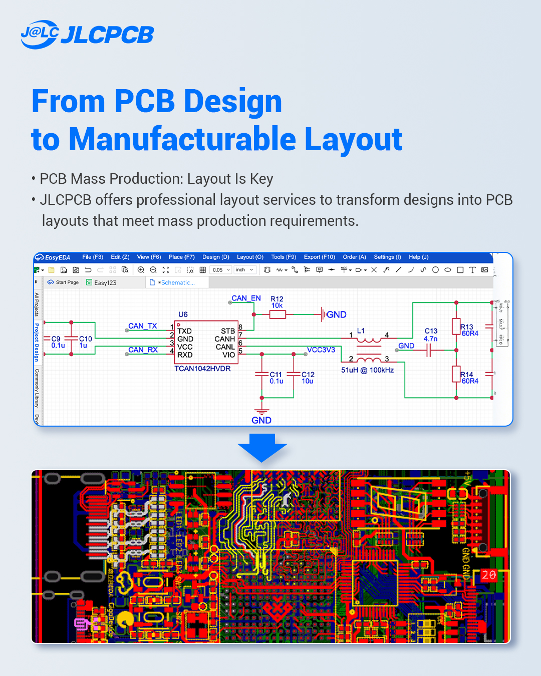
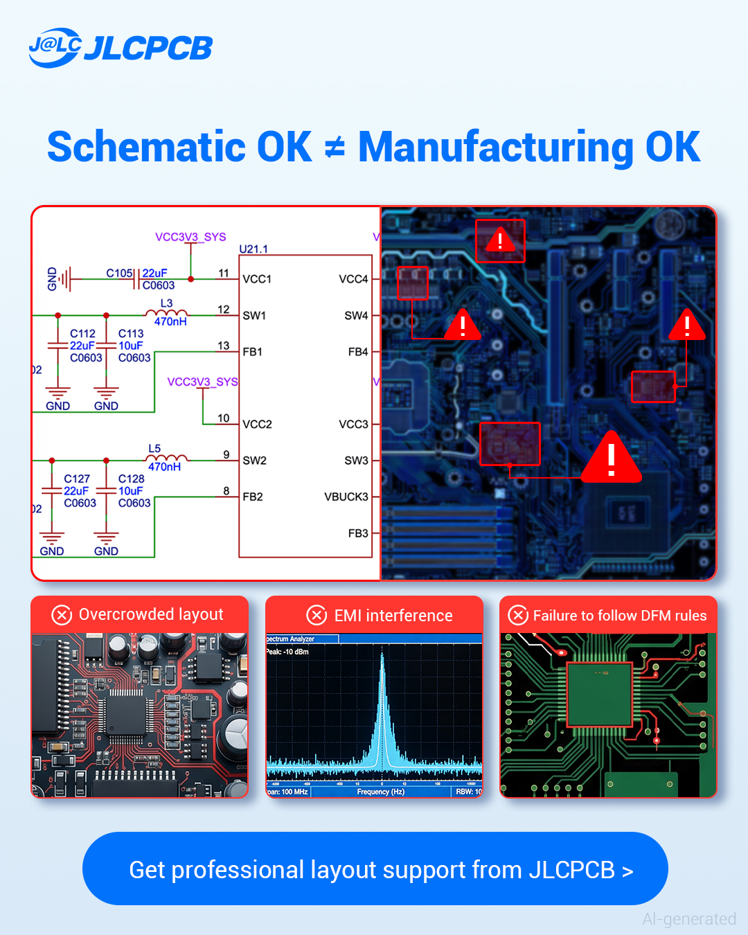
To give you a truly high-quality review of your EMI performance, I need you to export your PCB Layout file (the .json or Gerber files from EasyEDA) and send it to me. While the schematic looks great, the Layout is where the "Silent Power Rails" and "CAN Integrity" live or die. If I can see your trace routing, I can give you a "Pro" checklist on:
- Ground plane separation for the LIS3MDL.
- Differential pair routing for your CAN lines.
- Placement of your 22uF and 10kOhm components relative to high-speed lines.
Are you planning to run your LIS3MDL compass via the on-board I2C, or are you moving it to an external CAN node to get it further away from the motor interference?
Why CAN? (The Differential Advantage)
In many DIY builds, I2C is the default because it’s easy. However, I2C was designed for "chip-to-chip" communication on a single PCB, not for running wires across a drone frame. On a drone, long wires act like antennas, picking up massive electromagnetic interference (EMI) from your motors.
CAN (Controller Area Network) is different. It uses Differential Signaling. Instead of one signal wire, it uses two: CAN High (CANH) and CAN Low (CANL). The receiver only cares about the difference between them. If noise hits the wire, it usually hits both equally, and the difference remains the same.
CAN allows for four different message types. They are the data frame, remote frame, overload frame, and error frame. A standard CAN data frame makes use of the identifier, the data, and data length code, the cyclic redundancy check, and the acknowledgment bits. Both the RTR and IDE bits are dominant in data frames. If the recessive acknowledge bit at the receiving end is overwritten by a dominant bit, both the transmitter and receiver recognize this as a successful transmission.
A CAN remote frame looks similar to a data frame except for the fact that it does not contain any data. It is sent with the RTR bit in a recessive state; this indicates that it is a remote frame. Remote frames are used to request data from a node. When a node detects an error in a message on the CAN bus, it transmits an error frame. This results in all other nodes sending an error frame. Following this, the node where the error occurred retransmits the message. The overload frame works similarly but is used when a node is receiving frames faster than it can process them. This frame provides a time buffer so the node can catch up.

That figure shows a simplified version of a CAN transceiver's output and input. The '101' bitstream is coming from/going to a CAN controller and/or microcontroller. Notice that when the controller sends a stream of bits, these are complemented and placed on the CANH line. The CANL line is always the complement of CANH. For arbitration to work, a CAN device must monitor both what it is sending and what is currently on the bus, i.e., what it's receiving.

The figureshows both the CANH and CANL signals simultaneously so that you can see the CAN bus in action. Plotted below the bus signals is the differential voltage that corresponds to the dominant and recessive states of the CAN signals. The first three segments in time, t1–t3, are drawn to match up with the three bits shown above in Figure 5. We will look at this from the perspective of the output driver. The driver's input initially sees a '1' and complements this to a zero, which is placed on CANH. CANL sees the complement of CANH and goes high. This is shown as t1 in Figure 6. Notice that the CANH and CANL voltages are offset from one another. During time t1, CANH – CANL is very close to zero, since CANH and CANL are almost the same voltage. This period, where the driver is sending a logic '1' resulting in CANH and CANL being close to the same voltage, is what we call the CAN recessive state.
The next bit sent is a '0'. CANH gets its complement and CANL again gets the complement of CANH. Notice this time that the CANH and CANL voltages are not close to one another. Therefore, the differential voltage (VDIFF) is larger. This is the CAN dominant state. We say that the logic is inverted because a '1' takes the bus low and a '0' brings it high. The input receiver works in a similar fashion.
You can see the visual explanation of this noise rejection on the All About Circuits website in their Introduction to CAN Bus https://www.allaboutcircuits.com/technical-articles/introduction-to-can-controller-area-network/.
Drop a comment if you have ever had a "frozen" I2C bus mid-flight. it’s usually because of the noise.
The Hardware: Transceivers and Termination
Looking at your schematic, I see we’ve moved beyond simple logic levels. Your STM32 can't talk to the CAN bus directly; it needs a "translator" called a Transceiver.
The SN65HVD230 Transceiver

This chip converts the 3.3V digital signals from your MCU into the differential voltages required for the bus.
- Check the Datasheet: You should download the SN65HVD230 datasheet from Texas Instruments.
This diagram illustrates the typical application circuit from Reddit https://www.reddit.com/r/PrintedCircuitBoard/comments/jcgqch/sn65hvd230_can_transceiver_breakout/?rdt=61456
The 120Ohm Termination Rule
High-speed signals on a bus can "reflect" back when they hit the end of the wire, like a wave hitting a wall. This causes data corruption.
- The Fix: You MUST place a 120Ohm (2 x 60Ohm) resistor at the two physical ends of your bus.
- In your FC: I noticed your design includes a termination header. This is perfect.
How close is metal 3D printing to your life? This precisely custom watch band has the answer.
Made of BJ-316L stainless steel, it combines cutting-edge tech with premium style.
⚙️ "Support-Free" One-Piece Printing
🎯 High Hardness (HRC 25-30)
✨ Smooth & Precise
✨ Pro Polishing Service for a premium texture that feels great on your wrist.
🎁 Exclusive Gift for You:
Bring your metal designs to life! Get up to $47 in BJ-316L Coupons and start your project for as low as $5.
🚀 Claim your discount and quote now: 👉 https://jlc3dp.com/coupon-center?from=fiona
#JLC3DP# #Metal3DPrinting# #BJ316L# #StainlessSteel# #3DPrinting# #BinderJetting# #IndustrialDesign# #CustomWatchBand# #3DPrintedWatchBand# #3DPrintingCommunity# #3DPrintingMaterials# #3dprints#