JLCPCB Flexible Heater Routing Tool!

8715976417038708736

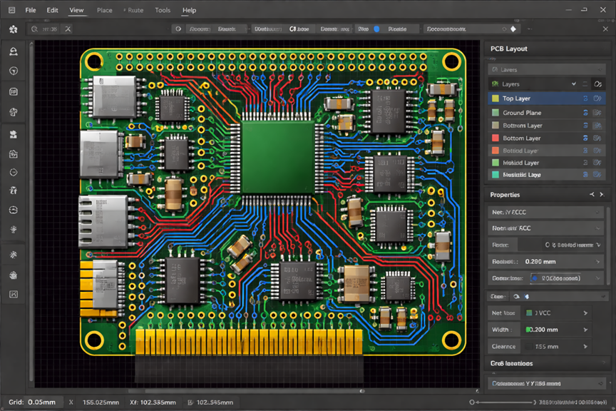
We are pleased to announce the release of the Flexible Heater Routing Tool!

You can access the tool via the following link:
https://jlcpcb-flexible-heater-routing-tool.netlify.app/

This tool enables you to independently verify whether your design meets the required specifications and is manufacturable, eliminating the need to wait until after order submission for validation. By using this tool, you can save valuable time and streamline your design process.

We encourage you to explore the tool and experience its benefits firsthand.

Flexible Heater
0.5mm BGA copper to hole clearance on inner layers

According to the BGA layout guidance, for 0.5mm pitch BGAs it is suggested to remove unused via pads on inner layers. https://jlcpcb.com/blog/bga-design-rules What is the minimum copper pour to drill-hole spacing for this on 6+ layer PCB with via-in-pad? And what is the minimum track to drill-hole spacing? Other pages state 0.2 mm but this wouldn't be compatible with routing on the inner layer as suggested in the BGA layout page. Example below with unused pads removed, and 0.12 mm hole to copper spacing in the photo.

image.png

PCB
Stop Fighting Your Solder Paste: The Secret to a Perfect First-Pass Yield 🛠️✨

We've all been there: you spend weeks perfecting a PCB layout, only to have the entire project sidelined by a bridge or a dry joint during reflow. Most of the time, the problem isn't your oven or your paste - it's the stencil.

If you're tired of "good enough" results and want professional-grade assembly without the professional-grade price tag, here is how JLCPCB Stencils are designed to help you succeed:

Precision That Actually Matters

We don't just "cut holes". We use over 30 high-precision laser cutting machines to ensure every aperture is burr-free and razor-sharp.

  • The Material: We use premium 304 HTA stainless steel.
  • The Accuracy: We maintain tolerances as tight as ±0.003mm. This level of precision is the difference between a clean solder "brick" and a messy smear that leads to shorts.
  • Pro Upgrades: Need even better release? Our electropolishing and nano-coating options significantly improve paste transfer efficiency and reduce bridging on fine-pitch components.

Speed That Keeps Up with Your Ideas

In the world of prototyping, time is your most valuable resource.

  • 12-Hour Production: Our fully automated lines can have your stencil ready in as little as 12 hours.
  • 24-Hour Shipping: Most orders are out the door within a day of confirmation.
  • Unbeatable Value: Professional precision starts at just $3 (100 × 100mm). You get tier-1 manufacturing quality on a maker's budget.

Your Design, Fully Supported

Every project is unique, so we don't limit your options. Whether you need a framed stencil for a production line or a frameless one for your bench, we've got you covered.

  • Advanced Options: From custom outlines and thicknesses to step stencils and ultrasonic-resistant adhesives, we support the complex modifications you need to turn your vision into a physical reality.

🚀 Upgrade Your Next Build for Less

At JLCPCB, were committed to helping you build faster and better. Don't let a low-quality stencil be the bottleneck of your next great invention.

SMT Stencil
3 Hassle-Free Ways to Order Your Precision Stencils at JLCPCB 🛠️📦

Whether you are starting a fresh project or realizing you forgot a stencil for an old board, we’ve made the ordering process incredibly flexible.

Depending on where you are in your design journey, here are the 3 easy ways to get your high-precision stencils:

Option 1: The "All-in-One" (PCB + Stencil Together)

8715558619110936576

This is the most popular choice for new projects. After you’ve configured your PCB parameters on our order page, simply scroll to the bottom and check the "Stencil" option. This ensures your stencil and PCBs are produced and shipped together, keeping your project perfectly synchronized.

Option 2: The "Stencil-Only" Sprint

8715558809674809344

Already have your boards but need a new stencil? No problem. Head to our website, click "Instant Quote," and select "SMT Stencil" from the top menu. You can upload your Gerber files and customize your stencil (Electropolished, Nano-coated, Frameless, etc.) in seconds.

Option 3: The "Oops, I Forgot!" (From Order History)

8715559002575450112

We've all been there—you ordered bare PCBs, and then realized hand-soldering those 0402s was a bad idea. Just go to your PCB Order History, find your previous order, click "Show all," and select "Need Stencil." We’ll generate a matching stencil for that exact board layout instantly.

🚀 Bring Your Designs to Life Faster & Better

At JLCPCB, we support your custom designs with the precision and convenience you need to succeed.

🎁 Click to Claim Your $11 Stencil Coupon Here! Experience the premium PCB stencil now!

✨ New User? Register now to unlock a $123 Coupon Bundle!

SMT Stencil
Are You Accidentally Ruining Your Stencils? 🛠️ 3 Essential Rules for Cleaning & Maintenance

A high-precision PCB stencil is an investment in a frustration-free assembly. But even the best electropolished stencil will fail if it's warped or clogged with dried-up paste. If you want to extend your stencil's lifespan and guarantee consistent, professional-grade printing every time you hit the bench, maintenance is non-negotiable.

Here are the industry-standard practices to keep your stencils in "day-one" condition:

Never Let Paste Sit 🧼

Don't allow solder paste to accumulate. Clean your stencils immediately after each use. Dried paste in the apertures—especially for fine-pitch components—is incredibly difficult to remove and is the #1 cause of "clogged" apertures during your next build.

Use the Right Solvents 🧪

Always use specified cleaning solvents (like IPA or dedicated stencil cleaners). Avoid harsh, non-approved chemicals that can degrade the surface tension of the metal or damage specialized nano-coatings. Using the correct cleaning solution protects the aperture integrity.

Store it Flat or Suffer the Warp 📏

Metal has a memory. Always lay your stencils flat when not in use. Storing them upright or leaning them against a wall can lead to subtle warping. A warped stencil won't sit flush against your PCB, leading to "smearing" and messy solder bridges.

🚀 Pro-Level Stencils for Your Next Project

At JLCPCB, we support your custom designs with high-precision manufacturing. Whether you need a standard laser-cut stencil or a premium nano-coated finish, we bring your designs to life so your assembly is faster and better.

💬Let's talk about how you maintain your gear. Drop your tips in the comments below! 👇

SMT Stencil
Why "Good Enough" Isn't Enough: A Deep Dive into PCB Stencil Precision

We've all been there: your PCB design is perfect, your components are ready, but after reflow, you're met with a nightmare of solder bridges and dry joints. Often, the culprit isn't your placement—it's a stencil that failed to meet the precision your design demanded. When you're dealing with fine-pitch components, a few microns are the difference between a working prototype and a pile of scrap.

Here is a technical breakdown of why precision is the heartbeat of stencil manufacturing:

The Need for High Precision

High precision in stencil manufacturing is vital for several reasons:

  1. Accurate Solder Paste Deposition: Precise apertures ensure the correct amount of solder paste is deposited, which is crucial for forming reliable solder joints.
  2. Minimized Solder Bridging: Accurate apertures reduce the risk of solder bridging between pads, which can cause short circuits.
  3. Consistent Quality: High precision stencils contribute to consistent quality across multiple boards, reducing defects and rework.

Example: JLCPCB Stencil with Small Pitch Components

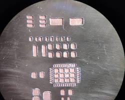
To illustrate the importance of high precision in stencil manufacturing, we ordered a PCB stencil from JLCPCB designed for a board with small pitch components. We will compare the desired dimensions of the stencil apertures with the actual manufactured dimensions using a digital microscope camera.

8715294814443917312

Measuring Precision with a Digital Microscope Camera

Using a digital microscope camera, we can capture high-resolution images of the stencil apertures and measure their dimensions. This allows us to verify the precision of the stencil manufacturing process.

Desired Dimensions vs. Actual Dimensions

For our example, we used a part MHPA0606RGBDT, which is a small LED with a pad size of 0.3mm x 0.3mm. Using a digital microscope camera, we will compare the desired dimensions of the stencil apertures with the actual manufactured dimensions.

Desired Dimensions:

· Pad Size: 0.3mm x 0.3mm

8715295063887429632

We will measure the actual dimensions of the stencil apertures for the MHPA0606RGBDT LED to ensure they match the desired specifications.

Results and Analysis

After capturing the images and measuring the apertures with the digital microscope camera, we found the following actual dimensions:

Actual Dimensions:

· Pad Size: 0.3098mm x 0.2980mm

These results show that the actual dimensions are very close to the desired dimensions, with only minor deviations. The deviations are within acceptable tolerances, demonstrating high precision in the stencil manufacturing process. This level of precision ensures accurate solder paste deposition, which is critical for the reliable performance of the assembled PCB.

8715295275162640384

🚀 Bring Your High-Density Designs to Life

At JLCPCB, we invest in the latest laser-cutting technology and inspection systems to ensure your custom designs are executed with microscopic accuracy. Whether you're working on 0201s or ultra-fine pitch ICs, we provide the precision you need to make your assembly faster and better.

SMT Stencil
From the Factory Floor: 4 Critical Stencil Manufacturing Tips to Save Your SMT Assembly 🛠️

The difference between a "good" stencil and a "perfect" one often comes down to the manufacturing choices you make before hitting that order button.

To ensure your PCB assembly is fast, clean, and defect-free, here are 4 Manufacturing Key Points we recommend focusing on:

Stencil Thickness Selection

The thickness of the design determines how much solder paste is applied. Focus primarily on the smallest pitch component on the board. Solder paste may adhere to the inner walls of the aperture in a thick stencil because of a phenomenon known as surface tension. A basic rule is that there should ideally be at least five solder particles in the smallest aperture.

8715288646241464320

Stencil Material

The type of material used to make the stencil will determine how well it removes solder paste from the apertures. Even though stainless steel is typically utilized, PCB designs that use fine pitch components can employ nickel, which is around 50% more expensive than stainless steel.

The first generation of stencils were made by chemical etching, which was effective for larger apertures but became increasingly challenging to remove solder from as component sizes decreased. This resulted in the creation of laser-cut stencils, which enhanced paste release by producing a much finer, trapezoidal-shaped aperture. As component sizes shrank, the potential for electropolishing the aperture walls and, later, the method of electro-forming the stencil were developed.

Apply Nano-Coating for Improved Paste Release

Hydrophobic coatings are used in contemporary nano-coated stencils to lessen solder paste adhesion to the aperture walls. This is essentially a straightforward procedure used to apply a layer of nanomaterial on a plain stencil. What is this layer going to do? It increases solder paste release, prolongs stencil life, and lowers cleaning frequency.

Consider Step Stencils for Mixed Assemblies

This is further divided into two parts:

Step-up stencils: Thicker regions for larger components.

Step-down stencils: Thinner regions for fine-pitch components.

It is used with boards having 0201 passive components and large connectors. We have covered a full detailed article on this topic, see from here.

🔥 Custom Precision, Powered by JLCPCB

At JLCPCB, we support full customization to turn your design into reality. Our high-precision manufacturing ensures your PCB assembly is completed faster, better, and with pro-grade results.

SMT Stencil
5 PCB Stencil Design Rules to Avoid Solder Bridges and Beads at the Source 🛠️

If your SMT assembly is plagued by solder bridges, mid-chip beads, or inconsistent deposits, the fix isn't just in your soldering iron - it's in the physics of your SMD stencil.

To achieve professional-grade results and prevent reflow defects, we explored 5 tips for your PCB Stencil design:

1. Aperture Design Guidelines

8715285886095966208

To prevent solder flaws like bridging and solder beads, this is crucial. For accurate deposition the apertures are made to be a bit smaller than the pads. However, for certain parts, an aperture with a specific design is required to deposit less paste on the inner edge of the part, which helps to prevent the formation of "mid-chip" solder balls. Here are a few instances:

8715286072646160384

Aperture Reduction (Pad-to-Aperture Ratio)

Apertures are frequently made slightly smaller than the actual pad dimensions in order to prevent bridging and extra solder. Here is a table of selection:

Recommended Thickness Rules:

For most components, the typical reduction is between 5 and 7%.

For dependable printability, IPC-7525 suggests a stencil-to-pad area ratio >0.66.

8715286304636768256

Formula:

Area Ratio = (Aperture Area) / (Aperture Wall Height × Aperture Perimeter)

Keep this ratio above 0.66 to ensure clean paste release.

Fiducial Marks

When printing solder paste onto pads, it is very important that the pattern is lined up correctly with the PCB. This is accomplished by applying fiducial marks, which are registration marks, to the PCB and stencil. As you can see from our most recent comprehensive piece on fiducial marks, adding them to the stencil will guarantee proper alignment. JLCPCB provides stencils with fiducial marks included, helping ensure accurate alignment and reliable solder paste printing.

8715286540696662016

Stencil Frame and Border

Stencils can be frameless (for rapid prototyping or manual printing) or framed (glued into aluminum frames).

8715286752165216256

Typical frame dimensions are 23 x 23 inches.

Keep the distance between the aperture area and the frame edge at least 10 mm.

Mark the stencil's position, thickness, and part number clearly.

Window Effect design

There are instances where the PCB design features big copper pads underneath the component. Devices that use power electronics typically experience this. In this case, a window effect is present to ensure a good electrical link and to let the device's heat escape. The device may lift and the outer leads may not solder if solder paste is placed over the entire pad. A "window effect" in the design can be used to decrease the solder volume, which is shared in the image above.

8715286980205465600

🚀 Turn Your Designs into Reality with JLCPCB

Whether it's a standard build or a complex custom project, we support your unique designs with high-precision stencils to make your SMT assembly faster, smoother, and more reliable.

SMT Stencil
Laser-Cut vs. Etched vs. Electroformed: Choosing the Right PCB Stencil 🛠️

If you're still hand-soldering SMD components pad-by-pad, you're playing life on "Hard Mode". Switching to a PCB Stencil and solder paste is the single biggest upgrade you can make for your workflow—but not all stencils are created equal.

Depending on your pitch size and budget, the manufacturing process matters. Here's the breakdown:

8715278740490657792

Chemical Etched Stencils (The "Old School" Choice)

These are made by using a chemical etchant to eat through the metal.

  • The Catch: The etching solution doesn't just go down; it goes sideways. This creates "undercutting," resulting in a slightly trapezoidal opening.
  • Best for: Large components and hobbyist projects where ultra-precision isn't a dealbreaker.

Laser-Cut Stencils (The Industry Standard)

This is the "sweet spot" for 99% of us. A CNC laser cuts the apertures with incredible accuracy.

  • The Perk: The laser naturally creates a slight inward taper. This actually helps the solder paste release cleanly from the stencil onto your board.
  • Best for: Most modern SMD designs, including QFNs and 0402s.

Electroformed Stencils (The Pro Tier)

These aren't "cut"—they are "grown" atom-by-atom through nickel plating.

  • The Perk: The walls are atom-level smooth. If you are dealing with ultra-fine pitch BGAs or 0201 components, this is the only way to ensure 100% consistent paste release.
  • Best for: High-density, professional-grade production.

🚀 Level Up Your Assembly

Ready to ditch the soldering iron and start stenciling? We've got you covered at JLCPCB.

SMT Stencil
SMT Stencil 101: How to Pick the Perfect SMT Stencil for Your PCB 🛠️

Buying a stencil seems simple, but the wrong specs can ruin your first-pass yield. To get a perfect solder finish every time, you need to master these three factors:

1. Thickness: The Volume Controller

The thickness determines exactly how much paste is deposited onto your pads.

  • The Rule: High-density boards with fine-pitch BGAs/QFNs (0.5mm pitch) require thinner stencils to avoid bridging. For larger components, go thicker for better joint strength.
  • Pro-Tip: If your board has mixed densities, you can adjust the "Solder Paste" layer in your CAD software (1:1 for general pitch, -10% for fine-pitch) to optimize paste volume without the high cost of localized thinning.

2. Material: Why Stainless Steel Wins

While copper is an option, Stainless Steel is the industry favorite for a reason.

  • Durability: It offers higher hardness and a much longer service life.
  • Precision: It's the best material for clean, burr-free laser cutting, ensuring the paste releases smoothly every single time.

3. Size: Framed vs. Frameless

Your stencil size is about more than just your PCB dimensions—it’s about your workflow.

  • Framed Stencils: Best for automated lines. Ensure the stencil outline matches your printer's mounting requirements.
  • Custom Frameless Stencils: Perfect for prototypes! If your board is under 10x10cm, don't waste money on a massive framed sheet.

Below this text you can find commonly used specifications and sizes at JLCPCB about framed stencil:

8715277607798296576

🚀 JLCPCB Advantage: We support customized sizes for frameless stencils starting at only $3! They are lightweight, easy to store, and can even ship with your PCBs to save on freight.

8715277750768861184

Quality assembly starts with the right stencil.

💰 Precision laser-cut stencils starting at $3!

🎁 Claim your $11 Coupon & $123 New User Rewards!

SMT Stencil
Are You Using the Right Stencil? 3 Types of SMT Stencil - Which one is your favorite?🧐

PCB assembly is a critical phase of any project. Whether you are hand-soldering at a workbench or running a fully automated SMT line, selecting the right stencil is crucial for a perfect finish.

Here are the three main types of SMT stencils, categorized by their application:

Framed SMT Stencils

8715275514697994240

What they are: Laser-cut foils permanently mounted in a rigid metal frame.

Best For: High-volume, automated SMT production lines.

The Edge: The frame provides the high, consistent tension required for machine alignment and repeatable precision over thousands of prints.

Frameless Stencils / Foils

8715275810135703552

What they are: Standalone stainless steel sheets without a fixed frame.

Best For: Prototyping, manual soldering, and small-batch DIY projects.

The Edge: Highly cost-effective and space-saving. Perfect for engineers using manual jigs or hand-printing methods.

Step Stencils

8715276012024737792

What they are: A specialized type where different areas of the stencil have varying thicknesses.

Best For: Complex boards mixing tiny, fine-pitch ICs with large, power-hungry components.

The Edge: Use "Step-up" or "Step-down" areas to precisely control solder volume for different components on the same board simultaneously.

Precision Made Simple with JLCPCB 🚀

Stop fighting with uneven solder paste and start getting perfect results. From quick prototypes to high-density production, we have the right tool for your process.

💰 Professional SMT stencils start at only $3!

🎁 Claim your $11 Coupon & $123 New User Rewards

How do you prefer to apply your paste? Manual or Machine? Let us know below! 👇

SMT Stencil
Solder 64 LEDs in Seconds? The "Cheat Code" for High-Density SMD Projects. 🚀

Dealing with high-density designs and tiny 0603 packages can be a nightmare for hand-soldering. But precision doesn't have to be slow. Whether you're a pro or a hobbyist, a JLCPCB SMT Stencil is the ultimate upgrade for your workbench.

8715274218263793664

As seen in this build by DIYGuyChris, a simple stainless steel stencil gives you consistent, perfect paste deposition across hundreds of pads instantly. Just Align, Swipe, and Lift—assembly has never been this smooth. Bring professional-grade soldering to your home projects!

💰 High quality, low price:

  • SMT Stencil starts at only $3
  • Order from just 1 piece

🎁 Click to get your $11 Coupon now!

SMT Stencil