DIY Current Meter using a Ferrite Core and Hall Sensor

I built a DC ammeter using a toroidal ferrite core and a Hall Effect sensor (WSH130NL). The idea is, when current flows through a wire around a toroidal core, it creates a magnetic field inside the core. For AC measurements we can just use a secondary winding and get a pretty good step down transformer producing an effective voltage which can be converted into current values. But with a DC steady signal we have to measure the magnetic flux in a different manner. Overall now with this approach we get an isolated current measurement. And by choosing the right number of windings, you can adjust the sensitivity and resolution of your ammeter to suit your needs. The same can be converted later with the help of a PCB provided by JLCPCB. As I got my MCU dev board fabricated from there in a $2 price. See the full article with code from here: https://www.hackster.io/sainisagar7294/diy-current-meter-using-a-ferrite-core-and-hall-sensor-4a91aa

8732326356871602176

How Does It Work?

When current passes through a conductor coiled around a toroidal ferrite core, it generates a magnetic field within the core. Due to the ferrite’s high permeability, the magnetic field is largely confined inside the core. By placing a Hall Effect sensor in the air gap, the sensor is positioned directly in the path of the magnetic flux. It then generates a voltage proportional to the magnetic field passing through it.

Components Required

WSH130NL Hall Effect Sensor

Toroidal Ferrite Core

Enamelled Copper Wire

10K Ohm Resistor

0.1uF Capacitor

Arduino Uno/Nano

16x2 LCD Display I2C

Building the DC Ammeter - Step by Step

The toroidal ferrite core is the heart of this ammeter. You can salvage one from an old power supply, a common-mode choke, or buy one online. The size doesn't matter too much, but a larger core gives you more room to wind wires.

Cutting the Air Gap:

This is the most critical and tricky step. We need to cut a small gap in the toroid where the Hall sensor will sit.

Winding the Toroid:

I used 10 turns of 24 AWG enamelled copper wire on a ferrite core. More windings mean a stronger magnetic field for the same current.

Placing the Hall Effect Sensor:

You can place the sensor, make sure it is flat in the middle of the gap, then secure it using hot glue and some tape. The orientation decides the polarity, but it doesn't matter even in this case because the steady state sensor readings are common mode by VDD/2.

Arduino Code:

The Arduino's 10-bit ADC gives us 1024 steps across 0-5V, which translates to approximately 4.88mV per step.

How to Calibrate:

  1. Upload the code to your Arduino with SENSITIVITY set to 0 initially
  2. With no current flowing, write down value of V_OFFSET.
  3. Pass a known current of say 1A and note the voltage.
  4. Pass another known current of 3A, note the voltage
  5. Update the V_OFFSET and SENSITIVITY defines in the code

Working:

At 0A:

8732326685126356992

At 1A:

8732326749445873664

At 2A:

8732326873350213632

At: 3A:

8732326927783485440

#HallEffect# #PCB# #currentmeter# #powermeter# #Arduino#

Test & Measurement
The Practicality of the Discrete Fourier Transform (DFT)

In typical applications of science and engineering, the Discrete Fourier Transform (DFT) stands as the most vital tool for digital signal processing. While other Fourier versions are essential for theoretical understanding, the DFT is uniquely suited for computer implementation. This is because both the time-domain sequence and its frequency-domain representation are discrete and finite. In my professional view, mastering the DFT is a mandatory requirement for any engineer working with digital systems and numerical algorithms.

The DFT allows you to analyze the frequency content of a signal with acceptable accuracy using finite computational resources. In my text, the analysis equation for a discrete sequence of length N is defined exactly as:

image.png

The practicality of this transform arises from the fact that it can be computed extremely fast using the Fast Fourier Transform (FFT) algorithm. This efficiency is what enables real-time spectral analysis in your drone communication links and radar systems. When you process a finite set of samples from an analog signal, you are essentially performing a DFT to understand its spectral characteristics.

By using the DFT, you can perform operations such as linear filtering and correlation in the frequency domain with much less arithmetic effort than in the time domain. This computational advantage is the primary reason why digital signal processing has revolutionized modern engineering. Mastering the properties and implementation of the DFT will provide you with a powerful analysis tool for your future projects in telecommunications and embedded systems.

image.png

The visualization shown comparison between a finite-length sequence and its corresponding discrete frequency spectrum.

Analog & Signal
The Four Versions of Fourier Analysis

In typical applications of science and engineering, we must choose the appropriate mathematical tool based on the characteristics of the signal we are processing. I believe that a clear understanding of the four versions of Fourier analysis is essential for your professional career in signal processing. These versions are distinguished primarily by whether the signal is continuous or discrete and whether it is periodic or aperiodic.

In my text, I classify these methods into four distinct categories. When you deal with continuous periodic signals, you utilize the Fourier Series (FS). If the signal is continuous and aperiodic, the Fourier Transform (FT) is the required tool. For your digital systems, we use the Discrete-Time Fourier Series (DTFS) for periodic sequences and the Discrete-Time Fourier Transform (DTFT) for aperiodic sequences.

The Discrete-Time Fourier Series is particularly important in digital engineering. The analysis equation for a discrete periodic signal with period N is defined exactly in my book as:

image.png

This equation allows you to determine the frequency components of a discrete signal with acceptable accuracy. It is crucial to remember that the properties of the signal in the time domain directly determine the properties of its representation in the frequency domain. For instance, periodicity in one domain always leads to discreteness in the other. Mastering this interplay will enable you to select the most efficient numerical algorithms for your specific engineering challenges.

image.png

these four versions based on time and frequency characteristics. (a) A periodic waveform; (b) its frequency-domain representation; (c) the frequency components of the waveform in (a); (d) the square error in approximating the waveform in (a) using only the dc component with different amplitudes.

image.png

(a)Samples at intervals of 1s, of a periodic continuous signal x(t) with period 5s;

(b)its scaled DFT spectrum;

(c)samples of x(t) at intervals of 0.125s;

(d)its scaled DFT spectrum.

The diagram illustrates the relationship between a periodic discrete signal and its corresponding frequency spectrum.

Analog & Signal
Impulse and Sinusoidal Signals

In typical applications of science and engineering, I believe that we must represent arbitrary signals in terms of simple and well-defined basic signals. The two most fundamental signals that you will encounter in your engineering career are the unit impulse and the sinusoidal signal. These signals serve as the building blocks for representing and processing more complex information.

The discrete unit impulse signal, which I denote as image.png
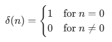
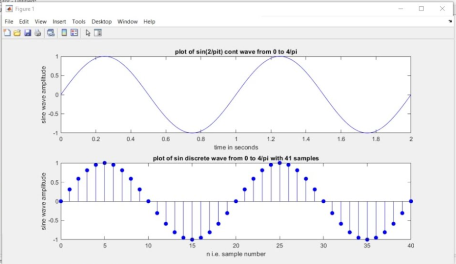
, is the simplest signal in discrete signal analysis. It is defined precisely in my text as:

image.png

This signal is essential because any arbitrary signal can be represented as a sum of shifted and scaled impulses. This representation is known as the sifting property of the impulse. By understanding the response of a system to a single impulse, you can effectively determine its response to any practical signal you might encounter.

Similarly, sinusoidal signals are crucial for frequency domain analysis. A discrete sinusoid is expressed with the following mathematical formula:

image.png

In my study of linear time invariant systems, sinusoidal signals are preferred because they are eigenfunctions of these systems. When you apply a sinusoidal input to a system, the output is also a sinusoid of the same frequency. This unique property allows us to characterize a system entirely by its frequency response. Mastering these basic signals is a vital prerequisite for all advanced signal processing tasks.

image.png

The illustration shows the discrete unit-impulse and unit-step signals clearly. 3 (a)The unit-impulse signal δ(n); (b)the unit-step signal u(n);(c)the unit-ramp signal r(n)

image.png

The waveforms a discrete sinusoid and its corresponding even and odd components.

Analog & Signal
Time-Domain vs. Frequency-Domain Analysis: A Brief Overview

In typical applications of science and engineering, we have to process signals using systems. In my signals and systems course, I focus on presenting two primary methods of analysis that are essential for your professional career. Time-domain analysis involves studying the variation of a signal amplitude as a function of time. This approach is highly intuitive because most practical signals are continuous functions of time, such as the telemetry data from your drone flight controllers.

Conversely, frequency-domain analysis allows us to look inside the signal to understand its spectral composition. I believe that a good grounding in frequency-domain methods is required to specialize in communication and signal processing. The transition between these domains is governed by Fourier analysis. For a discrete sequence of length N, the forward transformation is represented exactly in my text as:

image.png

By transforming your signals, you can analyze the frequency response of a system with acceptable accuracy. The major advantage of this shift is that operations like convolution in the time domain are replaced by simple multiplication in the frequency domain. This makes complex analysis much easier when designing filters or analyzing signal integrity. Mastering the interplay between these two domains is essential for modern engineers to choose the most efficient analysis method for any given practical problem.

image.png

The comprehensive overview the different versions of Fourier analysis depending on whether the signal is continuous or discrete.

(a) A periodic waveform; (b) its frequency-domain representation; (c) the frequency components of the waveform in (a); (d) the square error in approximating the waveform in (a) using only the dc component with different amplitudes

image.png

This visual demonstrates a periodic discrete sinusoid alongside its discrete-frequency spectrum.


Analog & Signal
Understanding Convolution in LTI System Analysis

In the analysis of linear time-invariant (LTI) systems, the most fundamental task involves determining the response of a system to an arbitrary input signal. My methodology emphasizes that if we possess the impulse response of a system, the output for any input can be calculated through the process of convolution. This operation serves as the definitive cornerstone of time-domain analysis in engineering.

Decomposing an input signal into a sum of weighted and shifted impulses allows us to compute the total output by summing the individual responses. For a discrete-time LTI system, the input-output relationship is defined by the convolution sum. In my text, this essential relationship is expressed exactly as:

image.png

The convolution process involves four primary mathematical steps: folding, shifting, multiplying, and summing. As you implement these steps in your design, you will observe how the impulse response characterizes the physical behavior of your hardware or signal processing algorithm.

image.png

The illustration provides a clear visualization of these operations. This specific image demonstrates the folding and shifting of the impulse response sequence relative to the input sequence. By examining this diagram, the graphical interpretation of the sum of products becomes intuitive for any engineer designing digital filters or drone communication protocols. Mastery of this tool is a vital prerequisite before you move toward complex frequency-domain representations.

Analog & Signal
Why Small Edge Features Matter More Than Many CNC Part Designs Show

In CNC machining, most design discussions focus on dimensions, tolerances, hole positions, thread depth, and surface finish. Those are obviously important, but many assembly and handling problems begin somewhere much smaller. The edge condition of a part, especially around holes and contact features, often decides whether a machined component feels clean and well-made or awkward and troublesome in real use.

This is one reason small edge features deserve more attention during design review. A part can be dimensionally correct and still create unnecessary problems if the entrance to a hole is too sharp, if burrs remain around a cut feature, or if repeated assembly quickly damages an untreated edge. These issues are easy to dismiss during CAD work because they do not look dramatic on the model. In production and assembly, they show up immediately.

A sharp hole entrance is a good example. On paper, the hole diameter may be perfect. In practice, a screw may start poorly, a pin may catch at the edge, or an operator may need to force the part into position. Once that happens, the edge is more likely to chip, deform, or raise a burr. The result is not just an ugly entrance. It becomes an assembly problem, and people often blame the fit or the tolerance before they look at the edge itself.

This is especially common on threaded holes, locating holes, and repeated-use features. A threaded hole may technically be correct, but if the entrance condition is rough or too sharp, fastener starting becomes less consistent. A locating pin may fit once but damage the hole mouth after repeated installation. On parts that are assembled and disassembled many times, the edge condition becomes part of the product’s real durability.

8731935949142949888

That is why controlled edge preparation matters. In many CNC parts, a very small edge treatment can reduce a much larger downstream problem. It may help guide entry, protect the feature during handling, reduce burr-related interference, and make the part feel more deliberate in assembly. This is not just about appearance. It is about how the part behaves.

The same principle applies to outer edges. A part does not need razor-sharp corners to be considered precise. In fact, sharp untreated corners are often less practical. They chip more easily, feel rougher in handling, and may create avoidable safety concerns during assembly or inspection. A controlled break at the edge often improves the part without affecting the design intent in any negative way.

Of course, not every edge needs the same treatment. Some edges only need a light break to remove sharpness. Others are functionally important and need a more deliberate feature to support alignment or entry. This is where machining knowledge becomes valuable. If every edge is treated casually, important features may remain under-controlled. If every edge is over-specified, cost and machining time go up without adding much value.

For designers and buyers, the practical question is not whether every part needs aggressive edge treatment. The real question is which edges affect function and which ones simply need to stop being sharp. Hole entrances, thread starts, locating features, and repeated assembly areas usually deserve more attention than random exterior corners.

This is also where communication on the drawing matters. General notes such as “break sharp edges” can be useful, but they are not always enough when the edge geometry affects assembly. A controlled entry feature should be treated differently from a casual deburred corner. If the edge is doing real work, the print should make that clear.

A good example of this thinking can be seen in the way chamfers are used on machined parts. A chamfer may look like a very small detail, but it often improves entry, protects edges, and reduces assembly frustration in ways that are easy to underestimate. A more detailed explanation of that topic can be found in this guide on chamfer in CNC machining: purpose, angles, applications, and drawing guide.

The broader lesson is simple. Small edge features are often treated like secondary details, but many of them influence how a part is actually used. In CNC machining, the difference between a part that merely passes inspection and a part that assembles cleanly, handles well, and lasts longer is sometimes found in those details.

When edge condition is reviewed early, many downstream problems become easier to prevent. Burrs are easier to control. Hole entry becomes smoother. Threads start more cleanly. Handling damage is reduced. Repeated assembly becomes more consistent. None of that changes the headline dimensions of the part, but it changes the real quality of the result.

For that reason, edge treatment should not be treated as an afterthought. It should be considered as part of how the design functions in production and in use. Small features often carry more value than they appear to on the drawing.

Design & Manufacturing
The Transition from Continuous to Digital Signal Processing

For most practical systems, input and output signals are continuous, and these signals can be processed using continuous systems. However, due to rapid advances in digital systems technology and fast numerical algorithms, it is highly advantageous to process continuous signals using digital systems by converting the input signal into a digital signal.

In my text, I always emphasize that a discrete signal is specified only at discrete values of its independent variable. For example, a continuous signal x(t) is represented only at t=nTs as x(nTs), where Ts is the sampling interval and n is an integer. The discrete signal is usually denoted as x(n), suppressing Ts in the argument of the function.

Consider the continuous complex exponential signal:

image.png

This mathematically well defined signal is predominantly used in signal and system analysis. To transition into the digital domain, we obtain the discrete signal by sampling the continuous signal, effectively replacing the variable t with nTs. Assuming a standard sampling interval, the discrete complex exponential signal elegantly becomes:

image.png

image.png

The graphical representation shown in your captured image perfectly visualizes the physical reality of replacing a continuous time variable with discrete mathematical steps.

Whether your discrete signal arises inherently or by sampling, the most important advantage is that it can be stored and processed efficiently using digital devices. This foundational transition from continuous to digital is precisely what enables the reliability of modern communication systems, ensuring that your RF transceivers and drone flight controllers operate with maximum computational efficiency.

Analog & Signal
Why Engineers Rely on Linear Time-Invariant (LTI) System Models

In typical applications of science and engineering, we have to process signals using systems. While most practical systems are nonlinear to some extent, they can be analyzed with acceptable accuracy by assuming linearity. In my experience, a good grounding in LTI system analysis is essential because it drastically simplifies our mathematical approach.

If we assume a system is Linear and Time Invariant, we unlock powerful analytical tools. The fundamental problem in the study of systems is how to analyze systems with arbitrary input signals. The solution, in the case of LTI systems, is to decompose the signal in terms of basic signals, such as the impulse or the sinusoid. Then, with knowledge of the response of a system to these basic signals, the response of the system to any arbitrary signal that you shall ever encounter in practice can be obtained.

For instance, using the convolution sum, the relationship between the input signal and the impulse response to find the output is defined perfectly as:

image.png

Furthermore, when dealing with complex exponential inputs, the relationship between the input and the output of an LTI system becomes a simple multiplication operation rather than a complex convolution. This mathematical property is exactly why we use it as the basis for signal decomposition. By mastering this assumption, your ability to design complex telemetry, control, and communication systems becomes incredibly efficient.

image.png

This diagram shown above perfectly illustrates how an arbitrary input is seamlessly processed by the characteristic impulse response of the system to generate a mathematically predictable output.

Analog & Signal
Designing UART Ports for RC Receivers and Telemetry (Part 2)

Designing the RCIN Port for Radio Control

The RCIN port is where your radio receiver connects to the flight system. This port faces very unique hardware challenges because it is frequently exposed to external elements and varying voltage levels from different receiver brands.

1. Absolute Input Protection with Zener Diodes

External modules are a primary source of hardware destruction. If a user accidentally injects a 5V power source into an RX pin that operates strictly at 3.3V, the event will permanently destroy the microcontroller.

To mitigate this catastrophic risk, I designed a dedicated hardware protection circuit on the RCIN header using a 10kOhm resistor, a 100 Ohm resistor, and a Zener diode. The Zener diode is placed in a reverse bias configuration between the signal line and Ground.

A Zener diode is a unique semiconductor that acts like a voltage pressure relief valve. During normal 3.3V operation, this diode is completely invisible to the signal. However, if a voltage spike exceeding 3.3V enters the pin, the Zener diode instantly activates and clamps the voltage, safely routing the dangerous excess energy straight to Ground. The 100 Ohm resistor acts as a current limiter to protect the diode from burning out, while the 10kOhm resistor provides a stable bias state.

image.png

For a deep academic explanation of how Zener diodes protect logic circuits, you can check on this website: Electronics Tutorials: Zener Diodes.

This images shown exactly how the diode is placed in parallel with the working load to clamp incoming voltage.)

image.png

2. The SBUS Inversion Advantage on the STM32H7

Legacy radio protocols like SBUS present a unique schematic challenge because SBUS is an inverted serial protocol. On a standard UART signal, an idle line is held HIGH and drops LOW to send data. SBUS does the exact opposite. On older generation Flight Controllers utilizing STM32F4 processors, hardware designers were forced to add complex external NPN transistor circuits to physically invert the signal before it reached the MCU.

However, my Flight Controller utilizes the exceptionally powerful STM32H7 processor. The STM32H7 features advanced internal UART peripherals that support direct hardware inversion via software configuration. Because of this, my schematic no longer requires an external logic inverter IC on the RCIN port. The raw inverted signal travels safely through our Zener protection network directly into the MCU. This saves valuable board space and reduces the number of components that could potentially fail in the air.

Software Integration via ArduPilot

Once the hardware is designed securely, we must configure the software to utilize these physical ports. Within ArduPilot firmware, every UART we route on the PCB is assigned a specific SERIAL number.

For the TELEME port, you must alter the SERIALx_PROTOCOL parameter in your Mission Planner software to activate MAVLink communication. For the RCIN port receiving the SBUS signal, we must command the STM32H7 processor to activate its internal hardware inverter. We accomplish this by modifying the SERIALx_OPTIONS parameter. By setting the correct bitmask, the processor will handle the SBUS inversion internally without any flaws.

You can check on this website for the official ArduPilot documentation regarding how to configure those specific serial options: ArduPilot Serial Options Documentation.

image.png

For a stunning visual explanation regarding how to design a UART hardware interface from start to finish, you can see in this video from Phil's Lab on YouTube: https://youtu.be/aVUqaB0IMh4?si=xleHFRQrn2qTWUUw

Conclusion

Designing the communication ports on a Flight Controller requires much more than simply drawing wires between component pins. By implementing proper 10uF and 100nF power filtering, utilizing 22 Ohm resistors for signal integrity, and designing a Zener diode network for absolute voltage protection, we guarantee that the drone will never lose connection to the pilot. Furthermore, leveraging the internal inversion capabilities of the STM32H7 processor allows us to create a much cleaner and more reliable circuit board.

Embedded Systems
Designing UART Ports for RC Receivers and Telemetry (Part 1)

Today, we are going to look specifically at the TELEME and RCIN blocks in my schematic. I will explain in detail how to design UART ports that are exceptionally robust. This design not only protects your microcontroller from physical electrical damage but also guarantees flawless data communication with your Radio Control receiver and your high power LoRa telemetry modules.

UART

image.png

Before we dissect the specific ports on the board, we must understand the underlying protocol. UART stands for Universal Asynchronous Receiver Transmitter. This protocol relies on two primary data lines, which are TX for Transmit and RX for Receive. When you connect any external module to the Flight Controller, you must always cross these communication lines. The TX pin of the external module connects to the RX pin of the Flight Controller, and the same rule applies in reverse.

image.png

If you want to understand the fundamental mechanics of serial communication at the hardware level, you can check on this website from SparkFun: SparkFun Serial Communication Tutorial. They offer a highly trusted explanation regarding how digital data packets are constructed and transmitted.

This images shown exactly how the internal shift registers handle the raw serial data stream.

image.png

Designing the TELEME Port for LoRa Telemetry

The TELEME port on my Flight Controller is designed specifically to connect to external radio telemetry modules. These modules are frequently high power LoRa radios that constantly broadcast flight data back to a laptop on the ground. Designing this port requires strict attention to power delivery stability and digital signal integrity.

1. Power Stability and Capacitive Filtering

Telemetry radios draw massive surges of current when they transmit data packets. If you power a 1 Watt radio directly from the same 5V line as your main MCU without adequate filtering, the rapid voltage drops will cause the microcontroller to reboot mid flight.

image.png

In my schematic, I ensure the TELEME port features a highly robust filter network. I implemented a 10uF bulk capacitor paired with a 100nF ceramic decoupling capacitor, placing both exactly next to the telemetry power pin. The 10uF capacitor acts as a localized energy reservoir to absorb the sudden current draw, while the 100nF capacitor actively filters out high frequency electrical noise. This combination guarantees the power plane remains absolutely stable.

2. Signal Integrity with 22 Ohm Resistors

High speed digital signals traveling across a printed circuit board can behave like radio waves. If the signal is too strong or the copper trace is too long, the signal will hit the end of the wire and bounce back. This creates reflections and ringing that corrupt the data integrity.

To prevent this, I placed a 22 Ohm series resistor on both the TX and RX lines at the TELEME port. This electrical technique is known as source termination. The 22 Ohm resistor absorbs the reflected energy and slightly slows down the rising edge of the digital signal. This approach heavily reduces electromagnetic interference and guarantees that your telemetry data reaches the LoRa module with maximum clarity.

You can check on this website for an outstanding academic discussion regarding how termination resistors work in digital electronics: Texas Instruments Termination Guide.

image.png

Embedded Systems
ESD Protection and VBUS Filtering in Flight Controllers - Part 2

PCB Routing: The Rules of High-Speed Data

Having the USBLC6-2P6 in your schematic is only 50 percent of the battle. The way you physically draw the copper traces on your PCB dictates whether the protection will actually work.

When laying out a Flight Controller, the USB data lines (D+ and D-) must be routed as a differential pair. This means the two copper traces must travel exactly parallel to each other, maintaining a strict 90 Ohm differential impedance. If you make one trace longer than the other, or if you space them incorrectly, the USB signal will bounce back and forth, causing your computer to say "USB Device Not Recognized."

Furthermore, the USBLC6-2P6 must be placed physically as close to the USB Type-C connector as humanly possible. If you place the protection diode near the microcontroller instead of the connector, the ESD spike will travel across the entire length of your circuit board, radiating massive electromagnetic interference into your gyroscopes and barometers before it finally gets clamped.

You must also never use a "via" (a hole that goes through the layers of the PCB) on the USB traces before they hit the protection diode. Vias add inductance, which slows down the clamping response time. The raw copper trace must go straight from the connector pin, into the diode pad, and then proceed to the MCU.

Drop a comment below if you want me to do a dedicated post on how to use your PCB layout software's impedance calculator to achieve the perfect 90 Ohm differential pair routing!

Hardware Defense Part 2: Taming the Noisy VBUS

Protecting the data communication lines ensures the brain of the drone can talk to the computer. But what about the power? We also need to carefully manage the 5V power coming from your computer cable, which is known on the schematic as VBUS.

Many people assume that the USB port on their expensive laptop outputs a perfectly clean, flat 5V DC signal. This is completely false. The 5V supplied by a standard PC motherboard or a cheap external USB hub is notoriously "dirty." It is generated by noisy switch-mode power supplies inside the computer, meaning the power is full of high-frequency noise, voltage ripples, and AC hum.

If we take this dirty 5V VBUS power and feed it directly into the Flight Controller's internal 3.3V Low Drop Out regulators, that noise does not just disappear. It bleeds straight through the regulator. This electrical noise will violently fluctuate the reference voltages used by the sensitive analog measurements of our gyros, accelerometers, and barometers. If you have ever plugged in your drone to Betaflight or ArduPilot and noticed your 3D model twitching randomly even though the drone is sitting perfectly still on your desk, dirty VBUS power is often the culprit!

The LC Pi-Filter Solution

To solve this noise problem and guarantee absolute stability, I designed a robust LC low-pass filter network specifically on the VBUS input line.

image.png

Before the raw 5V from the computer is allowed to reach the rest of the board (where it becomes the VBUS_IN net), it must pass through a gauntlet of components. The first component is an inductor, specifically a Ferrite Bead (labeled L1 on the schematic).

A ferrite bead is a fascinating component. At low frequencies (like pure DC power), it acts just like a normal piece of wire, allowing the 5V current to pass through freely. But at high frequencies (like the electrical noise generated by computer power supplies), the ferrite material actively resists the current. It literally absorbs the high-frequency electrical noise and safely dissipates it into the surrounding air as microscopic amounts of heat.

However, a ferrite bead alone is not enough. I combined this bead with two stages of capacitance. First, I placed a massive 10uF ceramic bulk capacitor. This acts as a localized energy reservoir, smoothing out any large voltage dips or low-frequency ripples from the computer. Second, I placed two 100nF ceramic decoupling capacitors directly adjacent to it. Because smaller capacitors have a lower Equivalent Series Resistance at high frequencies, the 100nF capacitors are perfectly tuned to absorb ultra-fast voltage spikes that the 10uF capacitor is too slow to catch.

Together, the Ferrite Bead, the 10uF capacitor, and the 100nF capacitors create an impenetrable LC filter. They take the chaotic, noisy power from your computer and transform it into a perfectly flat, clean, and safe 5V supply for the rest of your sensitive aviation hardware.

For an incredible visual explanation of how to design a robust USB hardware interface from scratch, including the math behind the TVS diodes and VBUS filtering we just discussed, you can see in this video from Phil's Lab on YouTube: https://youtu.be/W13HNsoHj7A?si=HAqM2yn2nMLlvtp2. He is a phenomenal resource for professional PCB design and watching him route these exact components is highly educational.

Embedded Systems